
Datasheet


© 2007-2012 Microchip Technology Inc. DS70292G-page 287
dsPIC33FJ32GP302/304, dsPIC33FJ64GPX02/X04, AND dsPIC33FJ128GPX02/X04
23.3 Comparator Voltage Reference
23.3.1 CONFIGURING THE COMPARATOR
VOLTAGE REFERENCE
The voltage reference module is controlled through the
CVRCON register (Register 23-2). The comparator
voltage reference provides two ranges of output
voltage, each with 16 distinct levels. The range to be
used is selected by the CVRR bit (CVRCON<5>). The
primary difference between the ranges is the size of the
steps selected by the CV
REF Selection bits
(CVR3:CVR0), with one range offering finer resolution.
The comparator reference supply voltage can come
from either V
DD and VSS, or the external VREF+ and
VREF-. The voltage source is selected by the CVRSS
bit (CVRCON<4>).
The settling time of the comparator voltage reference
must be considered when changing the CV
REF
output.
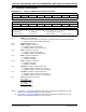
FIGURE 23-2: COMPARATOR VOLTAGE REFERENCE BLOCK DIAGRAM
16-to-1 MUX
8R
R
CVREN
CVRSS = 0
AV
DD
VREF+
CVRSS = 1
8R
CVRSS = 0
V
REF-
CVRSS = 1
R
R
R
R
R
R
16 Steps
CVRR
CVREF
CVR3
CVR2
CVR1
CVR0
CVRCON<3:0>
AV
SS
CVRSRC
CVROE (CVRCON<6>)
CVREFIN