
Datasheet


© 2007-2012 Microchip Technology Inc. DS70292G-page 285
dsPIC33FJ32GP302/304, dsPIC33FJ64GPX02/X04, AND dsPIC33FJ128GPX02/X04
23.2 Comparator Control Register
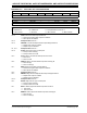
REGISTER 23-1: CMCON: COMPARATOR CONTROL REGISTER
R/W-0 U-0 R/W-0 R/W-0 R/W-0 R/W-0 R/W-0 R/W-0
CMIDL
— C2EVT C1EVT C2EN C1EN C2OUTEN
(1)
C1OUTEN
(2)
bit 15 bit 8
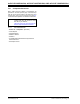
R-0 R-0 R/W-0 R/W-0 R/W-0 R/W-0 R/W-0 R/W-0
C2OUT C1OUT C2INV C1INV C2NEG C2POS C1NEG C1POS
bit 7 bit 0
Legend:
R = Readable bit W = Writable bit U = Unimplemented bit, read as ‘0’
-n = Value at POR ‘1’ = Bit is set ‘0’ = Bit is cleared x = Bit is unknown
bit 15 CMIDL: Stop in Idle Mode bit
1 = When device enters Idle mode, module does not generate interrupts. Module is still enabled.
0 = Continue normal module operation in Idle mode
bit 14 Unimplemented: Read as ‘0’
bit 13 C2EVT: Comparator 2 Event bit
1 = Comparator output changed states
0 = Comparator output did not change states
bit 12 C1EVT: Comparator 1 Event bit
1 = Comparator output changed states
0 = Comparator output did not change states
bit 11 C2EN: Comparator 2 Enable bit
1 = Comparator is enabled
0 = Comparator is disabled
bit 10 C1EN: Comparator 1 Enable bit
1 = Comparator is enabled
0 = Comparator is disabled
bit 9 C2OUTEN: Comparator 2 Output Enable bit
(1)
1 = Comparator output is driven on the output pad
0 = Comparator output is not driven on the output pad
bit 8 C1OUTEN: Comparator 1 Output Enable bit
(2)
1 = Comparator output is driven on the output pad
0 = Comparator output is not driven on the output pad
bit 7 C2OUT: Comparator 2 Output bit
When C2INV = 0:
1 =C2 VIN+ > C2 VIN-
0 =C2 V
IN+ < C2 VIN-
When C2INV =
1:
0 =C2 VIN+ > C2 VIN-
1 =C2 VIN+ < C2 VIN-
Note 1: If C2OUTEN = 1, the C2OUT peripheral output must be configured to an available RPx pin. See
Section 11.6 “Peripheral Pin Select” for more information.
2: If C1OUTEN = 1, the C1OUT peripheral output must be configured to an available RPx pin. See
Section 11.6 “Peripheral Pin Select” for more information.