
Datasheet


© 2007-2012 Microchip Technology Inc. DS70292G-page 275
dsPIC33FJ32GP302/304, dsPIC33FJ64GPX02/X04, AND dsPIC33FJ128GPX02/X04
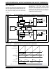
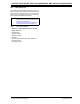
REGISTER 21-7: AD1CSSL: ADC1 INPUT SCAN SELECT REGISTER LOW
(1,2)
U-0 U-0 U-0 R/W-0 R/W-0 R/W-0 R/W-0 R/W-0
— — — CSS12 CSS11 CSS10 CSS9 CSS8
bit 15 bit 8
R/W-0 R/W-0 R/W-0 R/W-0 R/W-0 R/W-0 R/W-0 R/W-0
CSS7 CSS6 CSS5 CSS4 CSS3 CSS2 CSS1 CSS0
bit 7 bit 0
Legend:
R = Readable bit W = Writable bit U = Unimplemented bit, read as ‘0’
-n = Value at POR ‘1’ = Bit is set ‘0’ = Bit is cleared x = Bit is unknown
bit 15-12 Unimplemented: Read as ‘0’
bit 11-0 CSS<11:0>: ADC Input Scan Selection bits
1 = Select ANx for input scan
0 = Skip ANx for input scan
Note 1: On devices without 13 analog inputs, all AD1CSSL bits can be selected by the user application. However,
inputs selected for scan without a corresponding input on device converts V
REFL.
2: CSSx = ANx, where x = 0 through 12.
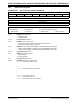
REGISTER 21-8: AD1PCFGL: ADC1 PORT CONFIGURATION REGISTER LOW
(1,2,3)
U-0 U-0 U-0 R/W-0 R/W-0 R/W-0 R/W-0 R/W-0
— — — PCFG12 PCFG11 PCFG10 PCFG9 PCFG8
bit 15 bit 8
R/W-0 R/W-0 R/W-0 R/W-0 R/W-0 R/W-0 R/W-0 R/W-0
PCFG7 PCFG6 PCFG5 PCFG4 PCFG3 PCFG2 PCFG1 PCFG0
bit 7 bit 0
Legend:
R = Readable bit W = Writable bit U = Unimplemented bit, read as ‘0’
-n = Value at POR ‘1’ = Bit is set ‘0’ = Bit is cleared x = Bit is unknown
bit 15-13 Unimplemented: Read as ‘0’
bit 12-0 PCFG<12:0>: ADC Port Configuration Control bits
1 = Port pin in Digital mode, port read input enabled, ADC input multiplexer connected to AV
SS
0 = Port pin in Analog mode, port read input disabled, ADC samples pin voltage
Note 1: On devices without 13 analog inputs, all PCFG bits are R/W by user software. However, the PCFG bits are
ignored on ports without a corresponding input on device.
2: PCFGx = ANx, where x = 0 through 12.
3: PCFGx bits have no effect if ADC module is disabled by setting ADxMD bit in the PMDx Register. In this
case all port pins multiplexed with ANx will be in Digital mode.