
Datasheet


dsPIC33FJ32GP302/304, dsPIC33FJ64GPX02/X04, AND dsPIC33FJ128GPX02/X04
DS70292G-page 272 © 2007-2012 Microchip Technology Inc.
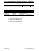
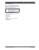
REGISTER 21-4: AD1CON4: ADC1 CONTROL REGISTER 4
U-0 U-0 U-0 U-0 U-0 U-0 U-0 U-0
— — — — — — — —
bit 15 bit 8
U-0 U-0 U-0 U-0 U-0 R/W-0 R/W-0 R/W-0
— — — — — DMABL<2:0>
bit 7 bit 0
Legend:
R = Readable bit W = Writable bit U = Unimplemented bit, read as ‘0’
-n = Value at POR ‘1’ = Bit is set ‘0’ = Bit is cleared x = Bit is unknown
bit 15-3 Unimplemented: Read as ‘0’
bit 2-0 DMABL<2:0>: Selects Number of DMA Buffer Locations per Analog Input bits
111 = Allocates 128 words of buffer to each analog input
110 = Allocates 64 words of buffer to each analog input
101 = Allocates 32 words of buffer to each analog input
100 = Allocates 16 words of buffer to each analog input
011 = Allocates 8 words of buffer to each analog input
010 = Allocates 4 words of buffer to each analog input
001 = Allocates 2 words of buffer to each analog input
000 = Allocates 1 word of buffer to each analog input