
Datasheet


dsPIC33FJ32GP302/304, dsPIC33FJ64GPX02/X04, AND dsPIC33FJ128GPX02/X04
DS70292G-page 258 © 2007-2012 Microchip Technology Inc.
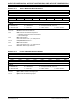
REGISTER 20-2: DCICON2: DCI CONTROL REGISTER 2
U-0 U-0 U-0 U-0 R/W-0 R/W-0 U-0 R/W-0
— — — — BLEN<1:0> —COFSG3
bit 15 bit 8
R/W-0 R/W-0 R/W-0 U-0 R/W-0 R/W-0 R/W-0 R/W-0
COFSG<2:0>
— WS<3:0>
bit 7 bit 0
Legend:
R = Readable bit W = Writable bit U = Unimplemented bit, read as ‘0’
-n = Value at POR ‘1’ = Bit is set ‘0’ = Bit is cleared x = Bit is unknown
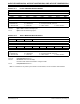
bit 15-12 Unimplemented: Read as ‘0’
bit 11-10 BLEN<1:0>: Buffer Length Control bits
11 = Four data words will be buffered between interrupts
10 = Three data words will be buffered between interrupts
01 = Two data words will be buffered between interrupts
00 = One data word will be buffered between interrupts
bit 9 Unimplemented: Read as ‘0’
bit 8-5 COFSG<3:0>: Frame Sync Generator Control bits
1111 = Data frame has 16 words
•
•
•
0010 = Data frame has 3 words
0001 = Data frame has 2 words
0000 = Data frame has 1 word
bit 4 Unimplemented: Read as ‘0’
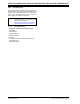
bit 3-0 WS<3:0>: DCI Data Word Size bits
1111 = Data word size is 16 bits
•
•
•
0100 = Data word size is 5 bits
0011 = Data word size is 4 bits
0010 = Invalid Selection. Do not use. Unexpected results may occur.
0001 = Invalid Selection. Do not use. Unexpected results may occur.
0000 = Invalid Selection. Do not use. Unexpected results may occur.