
Datasheet


dsPIC33FJ32GP302/304, dsPIC33FJ64GPX02/X04, AND dsPIC33FJ128GPX02/X04
DS70292G-page 24 © 2007-2012 Microchip Technology Inc.
3.4 Special MCU Features
The dsPIC33FJ32GP302/304, dsPIC33FJ64GPX02/
X04, and dsPIC33FJ128GPX02/X04 features a 17-bit
by 17-bit single-cycle multiplier that is shared by both
the MCU ALU and DSP engine. The multiplier can per-
form signed, unsigned and mixed-sign multiplication.
Using a 17-bit by 17-bit multiplier for 16-bit by 16-bit
multiplication not only allows you to perform mixed-sign
multiplication, it also achieves accurate results for
special operations, such as (-1.0) x (-1.0).
The dsPIC33FJ32GP302/304, dsPIC33FJ64GPX02/
X04, and dsPIC33FJ128GPX02/X04 supports 16/16
and 32/16 divide operations, both fractional and inte-
ger. All divide instructions are iterative operations. They
must be executed within a REPEAT loop, resulting in a
total execution time of 19 instruction cycles. The divide
operation can be interrupted during any of those
19 cycles without loss of data.
A 40-bit barrel shifter is used to perform up to a 16-bit
left or right shift in a single cycle. The barrel shifter can
be used by both MCU and DSP instructions.
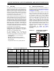
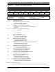
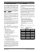
FIGURE 3-1: dsPIC33FJ32GP302/304, dsPIC33FJ64GPX02/X04, AND dsPIC33FJ128GPX02/
X04 CPU CORE BLOCK DIAGRAM
Instruction
Decode and
Control
PCH PCL
Program Counter
16-bit ALU
24
23
Instruction Reg
PCU
16 x 16
W Register Array
ROM Latch
EA MUX
Interrupt
Controller
Stack
Control
Logic
Loop
Control
Logic
Data Latch
Address
Latch
Control Signals
to Various Blocks
Literal Data
16
16
16
To Peripheral Modules
Data Latch
Address
Latch
16
X RAM
Y RAM
Address Generator Units
16
Y Data Bus
X Data Bus
DMA
Controller
DMA
RAM
DSP Engine
Divide Support
16
16
23
23
16
8
PSV and Table
Data Access
Control Block
16
16
16
16
Program Memory
Data Latch
Address Latch