
Datasheet


© 2007-2012 Microchip Technology Inc. DS70292G-page 203
dsPIC33FJ32GP302/304, dsPIC33FJ64GPX02/X04, AND dsPIC33FJ128GPX02/X04
15.0 OUTPUT COMPARE
The Output Compare module can select either Timer2
or Timer3 for its time base. The module compares the
value of the timer with the value of one or two compare
registers depending on the operating mode selected.
The state of the output pin changes when the timer
value matches the compare register value. The Output
Compare module generates either a single output
pulse or a sequence of output pulses, by changing the
state of the output pin on the compare match events.
The Output Compare module can also generate
interrupts on compare match events.
The Output Compare module has multiple operating
modes:
• Active-Low One-Shot mode
• Active-High One-Shot mode
• Toggle mode
• Delayed One-Shot mode
• Continuous Pulse mode
• PWM mode without Fault protection
• PWM mode with Fault protection
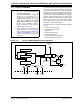
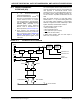
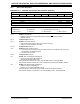
FIGURE 15-1: OUTPUT COMPARE MODULE BLOCK DIAGRAM
Note 1: This data sheet summarizes the features
of the dsPIC33FJ32GP302/304,
dsPIC33FJ64GPX02/X04, and
dsPIC33FJ128GPX02/X04 families of
devices. It is not intended to be a
comprehensive reference source. To
complement the information in this data
sheet, refer to Section 13. “Output
Compare” (DS70209) of the “dsPIC33F/
PIC24H Family Reference Manual”,
which is available from the Microchip
website (www.microchip.com).
2: Some registers and associated bits
described in this section may not be avail-
able on all devices. Refer to Section 4.0
“Memory Organization” in this data
sheet for device-specific register and bit
information.
OCxR
Comparator
Output
Logic
OCM<2:0>
OCx
Set Flag bit
OCxIF
OCxRS
Mode Select
3
0
1
OCTSEL
0
1
16
16
OCFA
TMR2
TMR2
QS
R
TMR3
TMR3
Rollover
Rollover
Output
Logic
Output
Enable
Enable