
Datasheet


dsPIC33FJ32GP302/304, dsPIC33FJ64GPX02/X04, AND dsPIC33FJ128GPX02/X04
DS70292G-page 166 © 2007-2012 Microchip Technology Inc.
11.9 Peripheral Pin Select Registers
The dsPIC33FJ32GP302/304, dsPIC33FJ64GPX02/
X04, and dsPIC33FJ128GPX02/X04 family of devices
implement 33 registers for remappable peripheral
configuration:
• 16 Input Remappable Peripheral Registers:
- RPINR0-RPINR1, RPINR3-RPINR4,
RPINR7, RPINR10-RPINR11 and
PRINR18-RPINR26
• 13 Output Remappable Peripheral Registers:
- RPOR0-RPOR12
Note: Input and Output Register values can only
be changed if the IOLOCK bit
(OSCCON<6>) is set to ‘0’. See
Section 11.6.3.1 “Control Register
Lock” for a specific command sequence.
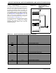
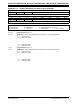
REGISTER 11-1: RPINR0: PERIPHERAL PIN SELECT INPUT REGISTER 0
U-0 U-0 U-0 R/W-1 R/W-1 R/W-1 R/W-1 R/W-1
— — —INT1R<4:0>
bit 15 bit 8
U-0 U-0 U-0 U-0 U-0 U-0 U-0 U-0
— — — — — — — —
bit 7 bit 0
Legend:
R = Readable bit W = Writable bit U = Unimplemented bit, read as ‘0’
-n = Value at POR ‘1’ = Bit is set ‘0’ = Bit is cleared x = Bit is unknown
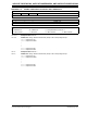
bit 15-13 Unimplemented: Read as ‘0’
bit 12-8 INT1R<4:0>: Assign External Interrupt 1 (INTR1) to the corresponding RPn pin
11111 = Input tied to V
SS
11001 = Input tied to RP25
•
•
•
00001 = Input tied to RP1
00000 = Input tied to RP0
bit 7-0 Unimplemented: Read as ‘0’