
Datasheet


dsPIC33FJ32GP302/304, dsPIC33FJ64GPX02/X04, AND dsPIC33FJ128GPX02/X04
DS70292G-page 150 © 2007-2012 Microchip Technology Inc.
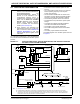
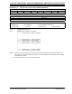
REGISTER 9-5: ACLKCON: AUXILIARY CONTROL REGISTER
(1)
U-0 U-0 R/W-0 R/W-0 R/W-0 R/W-0 R/W-0 R/W-0
— — SELACLK AOSCMD<1:0> APSTSCLR<2:0>
bit 15 bit 8
R/W-0 U-0 U-0 U-0 U-0 U-0 U-0 U-0
ASRCSEL
— — — — — — —
bit 7 bit 0
Legend:
R = Readable bit W = Writable bit U = Unimplemented bit, read as ‘0’
-n = Value at POR ‘1’ = Bit is set ‘0’ = Bit is cleared x = Bit is unknown
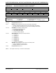
bit 15-14 Unimplemented: Read as ‘0’
bit 13 SELACLK: Select Auxiliary Clock Source for Auxiliary Clock Divider
1 = Auxiliary Oscillators provides the source clock for Auxiliary Clock Divider
0 = PLL output (Fosc) provides the source clock for the Auxiliary Clock Divider
bit 12-11 AOSCMD<1:0>: Auxiliary Oscillator Mode
11 = EC External Clock Mode Select
10 = XT Oscillator Mode Select
01 = HS Oscillator Mode Select
00 = Auxiliary Oscillator Disabled
bit 10-8 APSTSCLR<2:0>: Auxiliary Clock Output Divider
111 = divided by 1
110 = divided by 2
101 = divided by 4
100 = divided by 8
011 = divided by 16
010 = divided by 32
001 = divided by 64
000 = divided by 256 (default)
bit 7 ASRCSEL: Select Reference Clock Source for Auxiliary Clock
1 = Primary Oscillator is the Clock Source
0 = Auxiliary Oscillator is the Clock Source
bit 6-0 Unimplemented: Read as ‘0’
Note 1: This register is reset only on a Power-on Reset (POR).