
Datasheet


© 2007-2012 Microchip Technology Inc. DS70292G-page 141
dsPIC33FJ32GP302/304, dsPIC33FJ64GPX02/X04, AND dsPIC33FJ128GPX02/X04
9.0 OSCILLATOR CONFIGURATION
The dsPIC33FJ32GP302/304, dsPIC33FJ64GPX02/
X04, and dsPIC33FJ128GPX02/X04 oscillator system
provides:
• External and internal oscillator options as clock
sources
• An on-chip Phase-Locked Loop (PLL) to scale the
internal operating frequency to the required
system clock frequency
• An internal FRC oscillator that can also be used
with the PLL, thereby allowing full-speed operation
without any external clock generation hardware
• Clock switching between various clock sources
• Programmable clock postscaler for system power
savings
• A Fail-Safe Clock Monitor (FSCM) that detects
clock failure and takes fail-safe measures
• An Oscillator Control register (OSCCON)
• Non-volatile Configuration bits for main oscillator
selection
• An auxiliary crystal oscillator for Audio DAC
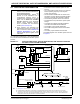
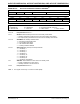
A simplified diagram of the oscillator system is shown
in Figure 9-1.
FIGURE 9-1: dsPIC33FJ32GP302/304, dsPIC33FJ64GPX02/X04, AND dsPIC33FJ128GPX02/
X04 OSCILLATOR SYSTEM DIAGRAM
Note 1: This data sheet summarizes the
features of the dsPIC33FJ32GP302/304,
dsPIC33FJ64GPX02/X04, and
dsPIC33FJ128GPX02/X04 families of
devices. It is not intended to be a
comprehensive reference source. To
complement the information in this data
sheet, refer to Section 39. “Oscillator
(Part III)” (DS70216) of the “dsPIC33F/
PIC24H Family Reference Manual”,
which is available from the Microchip
website (www.microchip.com).
2: Some registers and associated bits
described in this section may not be avail-
able on all devices. Refer to Section 4.0
“Memory Organization” in this data
sheet for device-specific register and bit
information.
Secondary Oscillator
LPOSCEN
SOSCO
SOSCI
Timer1
XTPLL, HSPLL,
XT, HS, EC
FRCDIV<2:0>
WDT, PWRT,
FSCM
FRCDIVN
SOSC
FRCDIV16
ECPLL, FRCPLL
NOSC<2:0> FNOSC<2:0>
Reset
FRC
Oscillator
LPRC
Oscillator
DOZE<2:0>
S3
S1
S2
S1/S3
S7
S6
FRC
LPRC
S0
S5
S4
÷16
Clock Switch
S7
Clock Fail
÷
2
TUN<5:0>
PLL
F
CY
(3)
FOSC
FRCDIV
DOZE
Note 1: See Figure 9-2 for PLL details.
2: If the Oscillator is used with XT or HS modes, an extended parallel resistor with the value of 1 MΩ must be connected.
3: The term F
P refers to the clock source for all the peripherals, while FCY refers to the clock source for the CPU. Throughout
this document F
CY and FP are used interchangeably, except in the case of Doze mode. FP and FCY will be different when
Doze mode is used in any ratio other than 1:1, which is the default.
÷N
ACLK
POSCCLK
Auxiliary Oscillator
SELACK
APSTSCLR<2:0>
DAC
FOSC
(1)
AOSCCLK
AOSCMD<1:0>
ASRCSEL
F
OSC
(1)
POSCCLK
OSC2
OSC1
Primary Oscillator
R
(2)
POSCMD<1:0>
FP
(3)
3.5 MHz ≤ AUX_OSC_FIN ≤ 10 MHz
1
0
0
1