dsPIC33FJ32GP302/304, dsPIC33FJ64GPX02/X04, and dsPIC33FJ128GPX02/X04 16-bit Digital Signal Controllers (up to 128 KB Flash and 16K SRAM) with Advanced Analog Operating Conditions System Peripherals • 3.0V to 3.6V, -40ºC to +150ºC, DC to 20 MIPS • 3.0V to 3.
dsPIC33FJ32GP302/304, dsPIC33FJ64GPX02/X04, AND dsPIC33FJ128GPX02/X04 dsPIC33FJ32GP302/304, dsPIC33FJ64GPX02/X04, AND dsPIC33FJ128GPX02/X04 PRODUCT FAMILIES The device names, pin counts, memory sizes, and peripheral availability of each device are listed below. The following pages show their pinout diagrams.
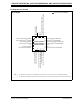
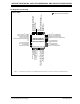
dsPIC33FJ32GP302/304, dsPIC33FJ64GPX02/X04, AND dsPIC33FJ128GPX02/X04 Pin Diagrams 28-Pin SPDIP, SOIC = Pins are up to 5V tolerant 1 28 AVDD 2 27 AVSS AN1/VREF-/CN3/RA1 3 26 AN9/DAC1LN/RP15(1)/CN11/PMCS1/RB15 25 AN10/DAC1LP/RTCC/RP14(1)/CN12/PMWR/RB14 24 AN11/DAC1RN/RP13(1)/CN13/PMRD/RB13 23 AN12/DAC1RP/RP12(1)/CN14/PMD0/RB12 PGED1/AN2/C2IN-/RP0(1)/CN4/RB0 4 PGEC1/ AN3/C2IN+/RP1(1)/CN5/RB1 5 (1) AN4/C1IN-/RP2 /CN6/RB2 (1) 6 AN5/C1IN+/RP3 /CN7/RB3 7 VSS 8 OSC1/CLKI/CN30/RA2 9 d
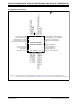
dsPIC33FJ32GP302/304, dsPIC33FJ64GPX02/X04, AND dsPIC33FJ128GPX02/X04 Pin Diagrams (Continued) 28-Pin QFN-S(2) AVDD AVSS AN9/DAC1LN/RP15(1)/CN11/PMCS1/RB15 AN10/DAC1LP/RTCC/RP14(1)/CN12/PMWR/RB14 24 23 22 28 PGED1/AN2/C2IN-/RP0(1)/CN4/RB0 (1) PGEC1/AN3/C2IN+/RP1 /CN5/RB1 AN4/C1IN-/RP2(1)/CN6/RB2 1 21 AN11/DAC1RN/RP13(1)/CN13/PMRD/RB13 2 20 AN12/DAC1RP/RP12(1)/CN14/PMD0/RB12 5 17 VCAP OSC1/CLKI/CN30/RA2 6 16 VSS OSC2/CLKO/CN29/PMA0/RA3 7 15 TDO/SDA1/RP9(1)/CN21/PMD3/RB9 14 PGED2/T
dsPIC33FJ32GP302/304, dsPIC33FJ64GPX02/X04, AND dsPIC33FJ128GPX02/X04 Pin Diagrams (Continued) 28-Pin QFN-S(2) AVSS AN9/DAC1LN/RP15(1)/CN11/PMCS1/RB15 24 23 22 AVDD 26 25 AN1/VREF-/CN3/RA1 AN0/VREF+/CN2/RA0 MCLR 28 27 AN10/DAC1LP/RTCC/RP14(1)/CN12/PMWR/RB14 = Pins are up to 5V tolerant PGED1/AN2/C2IN-/RP0(1)/CN4/RB0 1 21 AN11/RP13(1)/CN13/PMRD/RB13 PGEC1/AN3/C2IN+/RP1(1)/CN5/RB1 2 20 AN12/RP12(1)/CN14/PMD0/RB12 AN4/C1IN-/RP2(1)/CN6/RB2 PGED2/TDI/RP10(1)/CN16/PMD2/RB10 VSS 5 dsPIC33FJ12
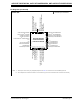
dsPIC33FJ32GP302/304, dsPIC33FJ64GPX02/X04, AND dsPIC33FJ128GPX02/X04 Pin Diagrams (Continued) 44-Pin QFN(2) PGEC1/AN3/C2IN+/RP1(1)/CN5/RB1 PGED1/AN2/C2IN-/RP0(1)/CN4/RB0 AN1/VREF-/CN3/RA1 AN0/VREF+/CN2/RA0 MCLR AVDD AVSS AN9/DAC1LN/RP15(1)/CN11/PMCS1/RB15 AN10/DAC1LP/RTCC/RP14(1)/CN12/PMWR/RB14 TCK/PMA7/RA7 TMS/PMA10/RA10 = Pins are up to 5V tolerant (1) AN5/C1IN+/RP3 /CN7/RB3 AN6/DAC1RM/RP16(1)/CN8/RC0 AN7/DAC1LM/RP17(1)/CN9/RC1 AN8/CVREF/RP18(1)/PMA2/CN10/RC2 11 AN11/DAC1RN/RP13(1)/CN13/PMRD/RB13
dsPIC33FJ32GP302/304, dsPIC33FJ64GPX02/X04, AND dsPIC33FJ128GPX02/X04 Pin Diagrams (Continued) 44-Pin QFN(2) AN4/C1IN-/RP2(1)/CN6/RB2 (1) AN5/C1IN+/RP3 /CN7/RB3 23 22 21 20 19 18 17 16 15 14 13 12 PGEC1/AN3/C2IN+/RP1(1)/CN5/RB1 PGED1/AN2/C2IN-/RP0(1)/CN4/RB0 AN1/VREF-/CN3/RA1 AN0/VREF+/CN2/RA0 MCLR AVDD AVSS AN9/RP15(1)/CN11/PMCS1/RB15 AN10/RTCC/RP14(1)/CN12/PMWR/RB14 TCK/PMA7/RA7 TMS/PMA10/RA10 = Pins are up to 5V tolerant 11 AN11/RP13(1)/CN13/PMRD/RB13 10 AN12/RP12(1)/CN14/PMD0/RB12 25 9 PGE
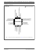
dsPIC33FJ32GP302/304, dsPIC33FJ64GPX02/X04, AND dsPIC33FJ128GPX02/X04 Pin Diagrams (Continued) 44-Pin TQFP 11 10 9 8 dsPIC33FJ64GP804 7 6 dsPIC33FJ128GP804 5 4 3 2 1 AN11/DAC1RN/RP13(1)/CN13/PMRD/RB13 AN12/DAC1RP/RP12(1)/CN14/PMD0/RB12 PGEC2/RP11(1)/CN15/PMD1/RB11 PGED2/EMCD2/RP10(1)/CN16/PMD2/RB10 VCAP VSS RP25(1)/CN19/PMA6/RC9 RP24(1)/CN20/PMA5/RC8 RP23(1)/CN17/PMA0/RC7 RP22(1)/CN18/PMA1/RC6 SDA1/RP9(1)/CN21/PMD3/RB9 34 35 36 37 38 39 40 41 42 43 44 23 24 25 26 27 28 29 30 31 32 33 SOSCO/T1CK/CN0/RA
dsPIC33FJ32GP302/304, dsPIC33FJ64GPX02/X04, AND dsPIC33FJ128GPX02/X04 Pin Diagrams (Continued) 44-Pin TQFP AN11/RP13(1)/CN13/PMRD/RB13 AN12/RP12(1)/CN14/PMD0/RB12 PGEC2/RP11(1)/CN15/PMD1/RB11 PGED2/EMCD2/RP10(1)/CN16/PMD2/RB10 VCAP VSS RP25(1)/CN19/PMA6/RC9 RP24(1)/CN20/PMA5/RC8 RP23(1)/CN17/PMA0/RC7 RP22(1)/CN18/PMA1/RC6 SDA1/RP9(1)/CN21/PMD3/RB9 34 35 36 37 38 39 40 41 42 43 44 11 23 10 24 25 9 8 26 27 dsPIC33FJ32GP304 7 28 dsPIC33FJ64GP204 6 5 29 dsPIC33FJ128GP204 4 30 3 31 2 32 1 33 SOSCO/T1CK/CN0/
dsPIC33FJ32GP302/304, dsPIC33FJ64GPX02/X04, AND dsPIC33FJ128GPX02/X04 Table of Contents dsPIC33FJ32GP302/304, dsPIC33FJ64GPX02/X04, and dsPIC33FJ128GPX02/X04 Product Families............................................. 2 1.0 Device Overview ........................................................................................................................................................................ 13 2.0 Guidelines for Getting Started with 16-bit Digital Signal Controllers .......................
dsPIC33FJ32GP302/304, dsPIC33FJ64GPX02/X04, AND dsPIC33FJ128GPX02/X04 TO OUR VALUED CUSTOMERS It is our intention to provide our valued customers with the best documentation possible to ensure successful use of your Microchip products. To this end, we will continue to improve our publications to better suit your needs. Our publications will be refined and enhanced as new volumes and updates are introduced.
dsPIC33FJ32GP302/304, dsPIC33FJ64GPX02/X04, AND dsPIC33FJ128GPX02/X04 Referenced Sources This device data sheet is based on the following individual chapters of the “dsPIC33F/PIC24H Family Reference Manual”. These documents should be considered as the general reference for the operation of a particular module or device feature. Note 1: To access the documents listed below, browse to the documentation section of the dsPIC33FJ64GP804 product page of the Microchip web site (www.microchip.
dsPIC33FJ32GP302/304, dsPIC33FJ64GPX02/X04, AND dsPIC33FJ128GPX02/X04 1.0 DEVICE OVERVIEW Note 1: This data sheet summarizes the features of the dsPIC33FJ32GP302/304, dsPIC33FJ64GPX02/X04, and dsPIC33FJ128GPX02/X04 families of devices. It is not intended to be a comprehensive reference source. To complement the information in this data sheet, refer to the “dsPIC33F/PIC24H Family Reference Manual”. Please see the Microchip web site (www.microchip.
dsPIC33FJ32GP302/304, dsPIC33FJ64GPX02/X04, AND dsPIC33FJ128GPX02/X04 FIGURE 1-1: dsPIC33FJ32GP302/304, dsPIC33FJ64GPX02/X04, AND dsPIC33FJ128GPX02/ X04 BLOCK DIAGRAM PSV and Table Data Access Control Block Y Data Bus X Data Bus Interrupt Controller 16 8 PORTA 16 16 16 Data Latch Data Latch X RAM Y RAM Address Latch Address Latch DMA RAM 23 23 PCU PCH PCL Program Counter Loop Stack Control Control Logic Logic PORTB 16 DMA 23 16 Controller 16 Address Generator Units Address Latch R
dsPIC33FJ32GP302/304, dsPIC33FJ64GPX02/X04, AND dsPIC33FJ128GPX02/X04 TABLE 1-1: PINOUT I/O DESCRIPTIONS Pin Type Buffer Type AN0-AN12 I Analog CLKI I ST/CMOS No CLKO O — No OSC1 I ST/CMOS No OSC2 I/O — No SOSCI SOSCO I O ST/CMOS — No No 32.768 kHz low-power oscillator crystal input; CMOS otherwise. 32.768 kHz low-power oscillator crystal output. CN0-CN30 I ST No No Change notification inputs. Can be software programmed for internal weak pull-ups on all inputs.
dsPIC33FJ32GP302/304, dsPIC33FJ64GPX02/X04, AND dsPIC33FJ128GPX02/X04 TABLE 1-1: PINOUT I/O DESCRIPTIONS (CONTINUED) Pin Type Buffer Type PPS SCL1 SDA1 ASCL1 ASDA1 I/O I/O I/O I/O ST ST ST ST No No No No Synchronous serial clock input/output for I2C1. Synchronous serial data input/output for I2C1. Alternate synchronous serial clock input/output for I2C1. Alternate synchronous serial data input/output for I2C1. TMS TCK TDI TDO I I I O ST ST ST — No No No No JTAG Test mode select pin.
dsPIC33FJ32GP302/304, dsPIC33FJ64GPX02/X04, AND dsPIC33FJ128GPX02/X04 TABLE 1-1: PINOUT I/O DESCRIPTIONS (CONTINUED) Pin Type Buffer Type PPS AVSS P P No Ground reference for analog modules. VDD P — No Positive supply for peripheral logic and I/O pins. VCAP P — No CPU logic filter capacitor connection. Vss P — No Ground reference for logic and I/O pins. VREF+ I Analog No Analog voltage reference (high) input. VREF- I Analog No Analog voltage reference (low) input.
dsPIC33FJ32GP302/304, dsPIC33FJ64GPX02/X04, AND dsPIC33FJ128GPX02/X04 NOTES: DS70292G-page 18 © 2007-2012 Microchip Technology Inc.
dsPIC33FJ32GP302/304, dsPIC33FJ64GPX02/X04, AND dsPIC33FJ128GPX02/X04 2.0 GUIDELINES FOR GETTING STARTED WITH 16-BIT DIGITAL SIGNAL CONTROLLERS Note 1: This data sheet summarizes the features of the dsPIC33FJ32GP302/304, dsPIC33FJ64GPX02/X04, and dsPIC33FJ128GPX02/X04 family of devices. It is not intended to be a comprehensive reference source. To complement the information in this data sheet, refer to the “dsPIC33F/PIC24H Family Reference Manual”, which is available from the Microchip website (www.
dsPIC33FJ32GP302/304, dsPIC33FJ64GPX02/X04, AND dsPIC33FJ128GPX02/X04 FIGURE 2-1: RECOMMENDED MINIMUM CONNECTION 0.1 µF Ceramic 10 µF Tantalum R R1 VSS VDD 2.4 VCAP VDD • Device Reset • Device programming and debugging C dsPIC33F VSS VDD VSS VDD AVSS VDD AVDD VSS 0.1 µF Ceramic 0.1 µF Ceramic 0.1 µF Ceramic L1(1) Note 1: As an option, instead of a hard-wired connection, an inductor (L1) can be substituted between VDD and AVDD to improve ADC noise rejection.
dsPIC33FJ32GP302/304, dsPIC33FJ64GPX02/X04, AND dsPIC33FJ128GPX02/X04 2.5 ICSP Pins 2.6 The PGECx and PGEDx pins are used for In-Circuit Serial Programming™ (ICSP™) and debugging purposes. It is recommended to keep the trace length between the ICSP connector and the ICSP pins on the device as short as possible. If the ICSP connector is expected to experience an ESD event, a series resistor is recommended, with the value in the range of a few tens of Ohms, not to exceed 100 Ohms.
dsPIC33FJ32GP302/304, dsPIC33FJ64GPX02/X04, AND dsPIC33FJ128GPX02/X04 TABLE 2-2: Part Number RESONATOR RECOMMENDATIONS Vendor Freq. Load Cap. FCR4.0M5T TDK Corp. 4 MHz N/A FCR8.0M5 TDK Corp. 8 MHz HWZT-10.00MD TDK Corp. 10 MHz HWZT-20.00MD TDK Corp. 20 MHz Legend: 2.7 Package Case Frequency Tolerance Mounting Type Operating Temperature Radial ±0.5% TH -40°C to +85°C N/A Radial ±0.5% TH -40°C to +85°C N/A Radial ±0.5% TH -40°C to +85°C N/A Radial ±0.
dsPIC33FJ32GP302/304, dsPIC33FJ64GPX02/X04, AND dsPIC33FJ128GPX02/X04 3.0 CPU Note 1: This data sheet summarizes the features of the dsPIC33FJ32GP302/304, dsPIC33FJ64GPX02/X04, and dsPIC33FJ128GPX02/X04 families of devices. It is not intended to be a comprehensive reference source. To complement the information in this data sheet, refer to Section 2. “CPU” (DS70204) of the “dsPIC33F/PIC24H Family Reference Manual”, which is available from the Microchip website (www.microchip.com).
dsPIC33FJ32GP302/304, dsPIC33FJ64GPX02/X04, AND dsPIC33FJ128GPX02/X04 3.4 Special MCU Features The dsPIC33FJ32GP302/304, dsPIC33FJ64GPX02/ X04, and dsPIC33FJ128GPX02/X04 supports 16/16 and 32/16 divide operations, both fractional and integer. All divide instructions are iterative operations. They must be executed within a REPEAT loop, resulting in a total execution time of 19 instruction cycles. The divide operation can be interrupted during any of those 19 cycles without loss of data.
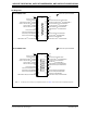
dsPIC33FJ32GP302/304, dsPIC33FJ64GPX02/X04, AND dsPIC33FJ128GPX02/X04 FIGURE 3-2: dsPIC33FJ32GP302/304, dsPIC33FJ64GPX02/X04, AND dsPIC33FJ128GPX02/ X04 PROGRAMMER’S MODEL D15 D0 W0/WREG PUSH.
dsPIC33FJ32GP302/304, dsPIC33FJ64GPX02/X04, AND dsPIC33FJ128GPX02/X04 3.5 CPU Resources Many useful resources are provided on the main product page of the Microchip web site for the devices listed in this data sheet. This product page, which can be accessed using this link, contains the latest updates and additional information. Note: 3.5.1 In the event you are not able to access the product page using the link above, enter this URL in your browser: http://www.microchip.com/wwwproducts/ Devices.
dsPIC33FJ32GP302/304, dsPIC33FJ64GPX02/X04, AND dsPIC33FJ128GPX02/X04 3.
dsPIC33FJ32GP302/304, dsPIC33FJ64GPX02/X04, AND dsPIC33FJ128GPX02/X04 REGISTER 3-1: SR: CPU STATUS REGISTER (CONTINUED) bit 7-5 IPL<2:0>: CPU Interrupt Priority Level Status bits(2) 111 = CPU Interrupt Priority Level is 7 (15), user interrupts disabled 110 = CPU Interrupt Priority Level is 6 (14) 101 = CPU Interrupt Priority Level is 5 (13) 100 = CPU Interrupt Priority Level is 4 (12) 011 = CPU Interrupt Priority Level is 3 (11) 010 = CPU Interrupt Priority Level is 2 (10) 001 = CPU Interrupt Priority Le
dsPIC33FJ32GP302/304, dsPIC33FJ64GPX02/X04, AND dsPIC33FJ128GPX02/X04 REGISTER 3-2: U-0 — bit 15 U-0 — R/W-0 SATB Legend: R = Readable bit 0’ = Bit is cleared bit 11 bit 10-8 U-0 — R/W-0 US R/W-0 EDT(1) R-0 R-0 DL<2:0> R-0 bit 8 R/W-0 SATA bit 7 bit 15-13 bit 12 CORCON: CORE CONTROL REGISTER R/W-1 SATDW R/W-0 ACCSAT C = Clear only bit W = Writable bit ‘x = Bit is unknown R/C-0 IPL3(2) R/W-0 PSV R/W-0 RND R/W-0 IF bit 0 -n = Value at POR ‘1’ = Bit is set U = Unimplemented bit, read as ‘
dsPIC33FJ32GP302/304, dsPIC33FJ64GPX02/X04, AND dsPIC33FJ128GPX02/X04 3.7 Arithmetic Logic Unit (ALU) 3.8 DSP Engine The dsPIC33FJ32GP302/304, dsPIC33FJ64GPX02/ X04, and dsPIC33FJ128GPX02/X04 ALU is 16 bits wide and is capable of addition, subtraction, bit shifts and logic operations. Unless otherwise mentioned, arithmetic operations are two’s complement in nature.
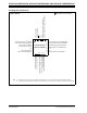
dsPIC33FJ32GP302/304, dsPIC33FJ64GPX02/X04, AND dsPIC33FJ128GPX02/X04 FIGURE 3-3: DSP ENGINE BLOCK DIAGRAM 40 S a 40 Round t 16 u Logic r a t e 40-bit Accumulator A 40-bit Accumulator B Carry/Borrow Out Carry/Borrow In Saturate Adder Negate 40 40 40 16 X Data Bus Barrel Shifter 40 Y Data Bus Sign-Extend 32 Zero Backfill 16 32 33 17-bit Multiplier/Scaler 16 16 To/From W Array © 2007-2012 Microchip Technology Inc.
dsPIC33FJ32GP302/304, dsPIC33FJ64GPX02/X04, AND dsPIC33FJ128GPX02/X04 3.8.1 MULTIPLIER The 17-bit x 17-bit multiplier is capable of signed or unsigned operation and can multiplex its output using a scaler to support either 1.31 fractional (Q31) or 32-bit integer results. Unsigned operands are zero-extended into the 17th bit of the multiplier input value. Signed operands are sign-extended into the 17th bit of the multiplier input value.
dsPIC33FJ32GP302/304, dsPIC33FJ64GPX02/X04, AND dsPIC33FJ128GPX02/X04 The Overflow and Saturation Status bits can optionally be viewed in the STATUS Register (SR) as the logical OR of OA and OB (in bit OAB) and the logical OR of SA and SB (in bit SAB). Programmers can check one bit in the STATUS register to determine if either accumulator has overflowed, or one bit to determine if either accumulator has saturated. This is useful for complex number arithmetic, which typically uses both accumulators.
dsPIC33FJ32GP302/304, dsPIC33FJ64GPX02/X04, AND dsPIC33FJ128GPX02/X04 3.8.3.2 Data Space Write Saturation 3.8.4 BARREL SHIFTER In addition to adder/subtracter saturation, writes to data space can also be saturated, but without affecting the contents of the source accumulator. The data space write saturation logic block accepts a 16-bit, 1.15 fractional value from the round logic block as its input, together with overflow status from the original source (accumulator) and the 16-bit round adder.
dsPIC33FJ32GP302/304, dsPIC33FJ64GPX02/X04, AND dsPIC33FJ128GPX02/X04 4.0 MEMORY ORGANIZATION Note: 4.1 This data sheet summarizes the features of the dsPIC33FJ32GP302/304, dsPIC33FJ64GPX02/X04, and dsPIC33FJ128GPX02/X04 families of devices. It is not intended to be a comprehensive reference source. To complement the information in this data sheet, refer to Section 4. “Program Memory” (DS70203) of the “dsPIC33F/ PIC24H Family Reference Manual”, which is available from the Microchip website (www.
dsPIC33FJ32GP302/304, dsPIC33FJ64GPX02/X04, AND dsPIC33FJ128GPX02/X04 4.1.1 PROGRAM MEMORY ORGANIZATION 4.1.2 All dsPIC33FJ32GP302/304, dsPIC33FJ64GPX02/ X04, and dsPIC33FJ128GPX02/X04 devices reserve the addresses between 0x00000 and 0x000200 for hard-coded program execution vectors. A hardware Reset vector is provided to redirect code execution from the default value of the PC on device Reset to the actual start of code.
dsPIC33FJ32GP302/304, dsPIC33FJ64GPX02/X04, AND dsPIC33FJ128GPX02/X04 4.2 Data Address Space The dsPIC33FJ32GP302/304, dsPIC33FJ64GPX02/ X04, and dsPIC33FJ128GPX02/X04 CPU has a separate 16-bit-wide data memory space. The data space is accessed using separate Address Generation Units (AGUs) for read and write operations. The data memory maps is shown in Figure 4-4. All Effective Addresses (EAs) in the data memory space are 16 bits wide and point to bytes within the data space.
dsPIC33FJ32GP302/304, dsPIC33FJ64GPX02/X04, AND dsPIC33FJ128GPX02/X04 FIGURE 4-3: DATA MEMORY MAP FOR dsPIC33FJ32GP302/304 DEVICES WITH 4 KB RAM MSB Address MSB 2 Kbyte SFR Space LSB Address 16 bits LSB 0x0000 0x0000 SFR Space 0x07FF 0x0801 0x07FE 0x0800 X Data RAM (X) 0x0FFE 0x1000 0x0FFF 0x1001 4 Kbyte SRAM Space Y Data RAM (Y) 0x13FE 0x1400 0x13FF 0x1401 0x17FF 0x1801 DMA RAM 0x8001 Optionally Mapped into Program Memory 0x17FE 0x1800 0x8000 X Data Unimplemented (X) 0xFFFF DS70292G-page
dsPIC33FJ32GP302/304, dsPIC33FJ64GPX02/X04, AND dsPIC33FJ128GPX02/X04 FIGURE 4-4: DATA MEMORY MAP FOR dsPIC33FJ128GP202/204 AND dsPIC33FJ64GP202/ 204 DEVICES WITH 8 KB RAM MSB Address MSB 2 Kbyte SFR Space LSB Address 16 bits LSB 0x0000 0x0001 SFR Space 0x07FE 0x0800 0x07FF 0x0801 8 Kbyte Near Data Space X Data RAM (X) 8 Kbyte SRAM Space 0x17FF 0x1801 0x1FFF 0x2001 0x27FF 0x2801 0x17FE 0x1800 Y Data RAM (Y) 0x1FFE 0x2000 DMA RAM 0x8001 0x27FE 0x2800 0x8000 X Data Unimplemented (X) Optionall
dsPIC33FJ32GP302/304, dsPIC33FJ64GPX02/X04, AND dsPIC33FJ128GPX02/X04 FIGURE 4-5: DATA MEMORY MAP FOR dsPIC33FJ128GP802/804 AND dsPIC33FJ64GP802/ 804 DEVICES WITH 16 KB RAM MSB Address 16 bits MSB 2 Kbyte SFR Space LSB Address LSB 0x0000 0x0001 SFR Space 0x07FF 0x0801 0x07FE 0x0800 X Data RAM (X) 16 Kbyte SRAM Space 0x1FFF 0x1FFE 0x27FF 0x2801 0x27FE 0x2800 0x3FFF 0x4001 0x47FF 0x4801 8 Kbyte Near Data Space Y Data RAM (Y) 0x3FFE 0x4000 DMA RAM 0x8001 0x47FE 0x4800 0x8000 X Data Unimpleme
dsPIC33FJ32GP302/304, dsPIC33FJ64GPX02/X04, AND dsPIC33FJ128GPX02/X04 4.2.5 X AND Y DATA SPACES The core has two data spaces, X and Y. These data spaces can be considered either separate (for some DSP instructions), or as one unified linear address range (for MCU instructions). The data spaces are accessed using two Address Generation Units (AGUs) and separate data paths.
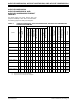
Special Function Register Maps TABLE 4-1: CPU CORE REGISTERS MAP © 2007-2012 Microchip Technology Inc.
CPU CORE REGISTERS MAP (CONTINUED) SFR Addr Bit 15 Bit 14 Bit 13 Bit 12 MODCON 0046 XMODEN YMODEN — — XMODSRT 0048 SFR Name Bit 11 Bit 10 Bit 9 Bit 8 Bit 7 BWM<3:0> Bit 6 Bit 5 YWM<3:0> XS<15:1> Bit 4 Bit 3 Bit 2 Bit 1 Bit 0 All Resets 0 xxxx XWM<3:0> 0000 XMODEND 004A XE<15:1> 1 xxxx YMODSRT 004C YS<15:1> 0 xxxx 1 xxxx YMODEND 004E XBREV 0050 BREN DISICNT 0052 — Legend: YE<15:1> XB<14:0> — Disable Interrupts Counter Register x = unknown value on Rese
CHANGE NOTIFICATION REGISTER MAP FOR dsPIC33FJ128GP202/802, dsPIC33FJ64GP202/802 AND dsPIC33FJ32GP302 SFR Name SFR Addr Bit 15 Bit 14 Bit 13 Bit 12 CNEN1 0060 CN15IE CN14IE CN13IE — CN30IE CN29IE CNEN2 0062 CNPU1 0068 CNPU2 006A Legend: Bit 11 Bit 10 Bit 9 CN12IE CN11IE — — — CN7IE — CN27IE — — CN24IE CN23IE — — — CN7PUE CN6PUE — — CN15PUE CN14PUE CN13PUE CN12PUE CN11PUE — CN30PUE CN29PUE — CN27PUE Bit 8 Bit 7 Bit 6 Bit 0 All Resets CN1IE CN0IE 0000 —
INTERRUPT CONTROLLER REGISTER MAP SFR Name SFR Addr Bit 15 Bit 14 INTCON1 0080 NSTDIS OVAERR INTCON2 0082 ALTIVT DISI Bit 13 Bit 12 Bit 11 OVBERR COVAERR COVBERR Bit 10 Bit 9 Bit 8 OVATE OVBTE COVTE — — — — — — Bit 7 Bit 6 Bit 5 Bit 4 Bit 3 Bit 2 Bit 1 Bit 0 — 0000 INT1EP INT0EP 0000 IC1IF INT0IF 0000 MI2C1IF SI2C1IF 0000 SFTACERR DIV0ERR DMACERR MATHERR ADDRERR STKERR OSCFAIL — — — — — INT2EP All Resets IFS0 0084 — DMA1IF AD1IF U1TXIF U1RXIF SPI1I
SFR Name SFR Addr TIMER REGISTER MAP Bit 15 Bit 14 Bit 13 Bit 12 Bit 11 Bit 10 Bit 9 Bit 8 Bit 7 Bit 6 Bit 5 Bit 4 Bit 3 Bit 2 Bit 1 Bit 0 All Resets TMR1 0100 Timer1 Register PR1 0102 Period Register 1 T1CON 0104 TMR2 0106 Timer2 Register 0000 TMR3HLD 0108 Timer3 Holding Register (for 32-bit timer operations only) xxxx TMR3 010A Timer3 Register 0000 PR2 010C Period Register 2 FFFF PR3 010E Period Register 3 T2CON 0110 TON — TSIDL — — — — — — TGATE T
SFR Name OUTPUT COMPARE REGISTER MAP SFR Addr Bit 15 Bit 14 Bit 13 Bit 12 Bit 11 Bit 10 Bit 9 Bit 8 Bit 7 Bit 6 OC1RS 0180 Output Compare 1 Secondary Register OC1R 0182 Output Compare 1 Register OC1CON 0184 OC2RS 0186 Output Compare 2 Secondary Register OC2R 0188 Output Compare 2 Register OC2CON 018A OC3RS 018C Output Compare 3 Secondary Register OC3R 018E Output Compare 3 Register OC3CON 0190 OC4RS 0192 Output Compare 4 Secondary Register OC4R 0194 Output Compare 4
SFR Name SFR Addr UART2 REGISTER MAP Bit 15 Bit 14 Bit 13 Bit 12 Bit 11 Bit 10 Bit 9 Bit 8 Bit 7 Bit 6 WAKE LPBACK Bit 5 Bit 4 Bit 3 ABAUD URXINV BRGH ADDEN RIDLE PERR Bit 2 Bit 1 All Resets STSEL 0000 URXDA 0110 U2MODE 0230 UARTEN — USIDL IREN RTSMD — UEN1 UEN0 U2STA 0232 UTXISEL1 UTXINV UTXISEL0 — UTXBRK UTXEN UTXBF TRMT U2TXREG 0234 — — — — — — — UTX8 UART Transmit Register xxxx U2RXREG 0236 — — — — — — — URX8 UART Receive Register
File Name Addr ADC1BUF0 0300 AD1CON1 0320 AD1CON2 0322 AD1CON3 0324 AD1CHS123 AD1CHS0 ADC1 REGISTER MAP FOR dsPIC33FJ64GP202/802, dsPIC33FJ128GP202/802 AND dsPIC33FJ32GP302 Bit 15 Bit 14 ADON — Bit 13 Bit 12 Bit 11 Bit 10 Bit 9 — AD12B FORM<1:0> — CSCNA CHPS<1:0> VCFG<2:0> — — — 0326 — — — 0328 CH0NB — — AD1PCFGL 032C — — — PCFG12 PCFG9 AD1CSSL 0330 — — — CSS12 CSS11 CSS10 CSS9 AD1CON4 0332 — — — — — — — Addr ADC1BUF0 0300 AD1CON1 0320 AD1C
File Name Addr DMA0CON DMA0REQ DMA0STA 0384 DMA REGISTER MAP Bit 15 Bit 14 Bit 13 Bit 12 Bit 11 Bit 10 Bit 9 Bit 8 Bit 7 Bit 6 0380 CHEN SIZE DIR HALF NULLW — — — — — 0382 FORCE — — — — — — — — Bit 5 Bit 4 AMODE<1:0> Bit 3 Bit 2 — — Bit 1 Bit 0 MODE<1:0> IRQSEL<6:0> All Resets 0000 0000 STA<15:0> 0000 0000 DMA0STB 0386 STB<15:0> DMA0PAD 0388 PAD<15:0> DMA0CNT 038A — — — — — — DMA1CON 038C CHEN SIZE DIR HALF NULLW — — — DMA1REQ 038E F
File Name Addr DMA5PAD 03C4 DMA5CNT DMA6CON DMA REGISTER MAP (CONTINUED) Bit 9 Bit 8 Bit 7 Bit 6 Bit 5 Bit 4 Bit 3 Bit 2 Bit 1 Bit 0 All Resets Bit 15 Bit 14 Bit 13 Bit 12 Bit 11 Bit 10 03C6 — — — — — — 03C8 CHEN SIZE DIR HALF NULLW — — — DMA6REQ 03CA FORCE — — — — — — — DMA6STA 03CC STA<15:0> 0000 DMA6STB 03CE STB<15:0> 0000 DMA6PAD 03D0 PAD<15:0> DMA6CNT 03D2 PAD<15:0> — — — — — — 0000 CNT<9:0> — — AMODE<1:0> — 0000 — — MODE<1:0>
File Name ECAN1 REGISTER MAP WHEN C1CTRL1.
File Name ECAN1 REGISTER MAP WHEN C1CTRL1.
File Name ECAN1 REGISTER MAP WHEN C1CTRL1.
PERIPHERAL PIN SELECT INPUT REGISTER MAP File Name Addr Bit 15 Bit 14 Bit 13 RPINR0 0680 — — — RPINR1 0682 — — — RPINR3 0686 — — — RPINR4 0688 — — RPINR7 068E — RPINR10 0694 — RPINR11 0696 RPINR18 Bit 12 Bit 11 — — Bit 10 Bit 9 Bit 8 — — Bit 2 Bit 1 Bit 0 All Resets — — — 1F00 Bit 7 Bit 6 Bit 5 Bit 4 Bit 3 — — — — — — — — INT2R<4:0> 001F T3CKR<4:0> — — — T2CKR<4:0> 1F1F — T5CKR<4:0> — — — T4CKR<4:0> 1F1F — — IC2R<4:0> — — —
PERIPHERAL PIN SELECT OUTPUT REGISTER MAP FOR dsPIC33FJ128GP202/802, dsPIC33FJ64GP202/802 AND dsPIC33FJ32GP302 File Name Addr Bit 15 Bit 14 Bit 13 RPOR0 06C0 — — — RPOR1 06C2 — — RPOR2 06C4 — — RPOR3 06C6 — RPOR4 06C8 RPOR5 06CA RPOR6 06CC RPOR7 Legend: Bit 11 Bit 10 Bit 9 Bit 8 Bit 4 Bit 3 Bit 2 Bit 1 Bit 0 All Resets Bit 7 Bit 6 Bit 5 RP1R<4:0> — — — RP0R<4:0> 0000 — RP3R<4:0> — — — RP2R<4:0> 0000 — RP5R<4:0> — — — RP4R<4:0> 0000 — — RP7R<4:0
File Name PARALLEL MASTER/SLAVE PORT REGISTER MAP FOR dsPIC33FJ128GP202/802, dsPIC33FJ64GP202/802 AND dsPIC33FJ32GP302 Addr Bit 15 Bit 14 Bit 13 PMCON 0600 PMPEN — PSIDL PMMODE 0602 BUSY PMADDR PMDOUT1 0604 ADDR15 IRQM<1:0> Bit 12 Bit 11 Bit 10 Bit 9 Bit 8 ADRMUX<1:0> PTBEEN PTWREN PTRDEN INCM<1:0> MODE16 MODE<1:0> CS1 Bit 7 Bit 6 Bit 5 Bit 4 Bit 3 Bit 2 Bit 1 Bit 0 All Resets CSF1 CSF0 ALP — CS1P BEP WRSP RDSP 0000 WAITB<1:0> WAITM<3:0> WAITE<1:0> ADDR<13:
File Name Addr REAL-TIME CLOCK AND CALENDAR REGISTER MAP Bit 15 Bit 14 ALRMEN CHIME ALRMVAL 0620 ALCFGRPT 0622 RTCVAL 0624 RCFGCAL 0626 RTCEN — PADCFG1 02FC — — Legend: Bit 12 Bit 11 Bit 10 Bit 9 Bit 8 Bit 7 Bit 6 Bit 5 Bit 4 Bit 3 Bit 2 Bit 1 Bit 0 Alarm Value Register Window based on APTR<1:0> AMASK<3:0> xxxx ALRMPTR<1:0> ARPT<7:-0> 0000 RTCC Value Register Window based on RTCPTR<1:0> RTCWREN RTCSYNC HALFSEC — — RTCOE — xxxx RTCPTR<1:0> — — CAL<7:0> — — Al
File Name Addr PORTA REGISTER MAP FOR dsPIC33FJ128GP204/804, dsPIC33FJ64GP204/804 AND dsPIC33FJ32GP304 Bit 15 Bit 14 Bit 13 Bit 12 Bit 11 Bit 10 Bit 9 Bit 8 Bit 7 Bit 6 Bit 5 Bit 4 Bit 3 Bit 2 Bit 1 Bit 0 All Resets TRISA 02C0 — — — — — TRISA10 TRISA9 TRISA8 TRISA7 — — TRISA4 TRISA3 TRISA2 TRISA1 TRISA0 079F PORTA 02C2 — — — — — RA10 RA9 RA8 RA7 — — RA4 RA3 RA2 RA1 RA0 xxxx LATA 02C4 — — — — — LATA10 LATA9 LATA8 LATA7 — — LATA4 LATA3 LA
SYSTEM CONTROL REGISTER MAP File Name Addr Bit 15 Bit 14 Bit 13 Bit 12 Bit 11 Bit 10 Bit 9 Bit 8 Bit 7 Bit 6 Bit 5 Bit 4 Bit 3 Bit 2 Bit 1 Bit 0 All Resets RCON 0740 TRAPR IOPUWR — — — — CM VREGS EXTR SWR SWDTEN WDTO SLEEP IDLE BOR POR xxxx(1) OSCCON 0742 — CLKLOCK IOLOCK LOCK — CF — LPOSCEN OSWEN 0300(2) CLKDIV 0744 ROI PLLFBD 0746 — — OSCTUN 0748 — — — ACLKCON 074A — — SELACLK Legend: Note 1: 2: x = unknown value on Reset, — = unimplemen
dsPIC33FJ32GP302/304, dsPIC33FJ64GPX02/X04, AND dsPIC33FJ128GPX02/X04 4.4.1 SOFTWARE STACK 4.4.2 In addition to its use as a working register, the W15 register in the dsPIC33FJ32GP302/304, dsPIC33FJ64GPX02/X04, and dsPIC33FJ128GPX02/ X04 devices is also used as a software Stack Pointer. The Stack Pointer always points to the first available free word and grows from lower to higher addresses. It pre-decrements for stack pops and post-increments for stack pushes, as shown in Figure 4-6.
dsPIC33FJ32GP302/304, dsPIC33FJ64GPX02/X04, AND dsPIC33FJ128GPX02/X04 TABLE 4-37: FUNDAMENTAL ADDRESSING MODES SUPPORTED Addressing Mode File Register Direct Description The address of the file register is specified explicitly. Register Direct The contents of a register are accessed directly. Register Indirect The contents of Wn forms the Effective Address (EA). Register Indirect Post-Modified The contents of Wn forms the EA. Wn is post-modified (incremented or decremented) by a constant value.
dsPIC33FJ32GP302/304, dsPIC33FJ64GPX02/X04, AND dsPIC33FJ128GPX02/X04 4.6 Modulo Addressing Modulo Addressing mode is a method of providing an automated means to support circular data buffers using hardware. The objective is to remove the need for software to perform data address boundary checks when executing tightly looped code, as is typical in many DSP algorithms. Modulo Addressing can operate in either data or program space (since the data pointer mechanism is essentially the same for both).
dsPIC33FJ32GP302/304, dsPIC33FJ64GPX02/X04, AND dsPIC33FJ128GPX02/X04 4.6.3 MODULO ADDRESSING APPLICABILITY Modulo Addressing can be applied to the Effective Address (EA) calculation associated with any W register.
dsPIC33FJ32GP302/304, dsPIC33FJ64GPX02/X04, AND dsPIC33FJ128GPX02/X04 FIGURE 4-8: BIT-REVERSED ADDRESS EXAMPLE Sequential Address b15 b14 b13 b12 b11 b10 b9 b8 b7 b6 b5 b4 b3 b2 b1 0 Bit Locations Swapped Left-to-Right Around Center of Binary Value b15 b14 b13 b12 b11 b10 b9 b8 b7 b6 b5 b1 b2 b3 b4 0 Bit-Reversed Address Pivot Point TABLE 4-38: XB = 0x0008 for a 16-Word Bit-Reversed Buffer BIT-REVERSED ADDRESS SEQUENCE (16-ENTRY) Normal Address Bit-Reversed Address A3 A2 A1 A0 Decimal A3
dsPIC33FJ32GP302/304, dsPIC33FJ64GPX02/X04, AND dsPIC33FJ128GPX02/X04 4.8 Interfacing Program and Data Memory Spaces 4.8.1 Since the address ranges for the data and program spaces are 16 and 24 bits, respectively, a method is needed to create a 23-bit or 24-bit program address from 16-bit data registers. The solution depends on the interface method to be used.
dsPIC33FJ32GP302/304, dsPIC33FJ64GPX02/X04, AND dsPIC33FJ128GPX02/X04 FIGURE 4-9: DATA ACCESS FROM PROGRAM SPACE ADDRESS GENERATION Program Counter(1) Program Counter 0 0 23 bits EA Table Operations(2) 1/0 1/0 TBLPAG 8 bits 16 bits 24 bits Select Program Space Visibility(1) (Remapping) 0 1 EA 0 PSVPAG 8 bits 15 bits 23 bits User/Configuration Space Select Byte Select Note 1: The Least Significant bit (LSb) of program space addresses is always fixed as ‘0’ to maintain word alignment of da
dsPIC33FJ32GP302/304, dsPIC33FJ64GPX02/X04, AND dsPIC33FJ128GPX02/X04 4.8.2 DATA ACCESS FROM PROGRAM MEMORY USING TABLE INSTRUCTIONS The TBLRDL and TBLWTL instructions offer a direct method of reading or writing the lower word of any address within the program space without going through data space. The TBLRDH and TBLWTH instructions are the only method to read or write the upper 8 bits of a program space word as data. The PC is incremented by two for each successive 24-bit program word.
dsPIC33FJ32GP302/304, dsPIC33FJ64GPX02/X04, AND dsPIC33FJ128GPX02/X04 4.8.3 READING DATA FROM PROGRAM MEMORY USING PROGRAM SPACE VISIBILITY The upper 32 Kbytes of data space may optionally be mapped into any 16K word page of the program space. This option provides transparent access to stored constant data from the data space without the need to use special instructions (such as TBLRDL/H).
dsPIC33FJ32GP302/304, dsPIC33FJ64GPX02/X04, AND dsPIC33FJ128GPX02/X04 NOTES: DS70292G-page 70 © 2007-2012 Microchip Technology Inc.
dsPIC33FJ32GP302/304, dsPIC33FJ64GPX02/X04, AND dsPIC33FJ128GPX02/X04 5.0 FLASH PROGRAM MEMORY programming data (one of the alternate programming pin pairs: PGECx/PGEDx), and three other lines for power (VDD), ground (VSS) and Master Clear (MCLR). This allows customers to manufacture boards with unprogrammed devices and then program the digital signal controller just before shipping the product. This also allows the most recent firmware or a custom firmware to be programmed.
dsPIC33FJ32GP302/304, dsPIC33FJ64GPX02/X04, AND dsPIC33FJ128GPX02/X04 5.2 RTSP Operation The dsPIC33FJ32GP302/304, dsPIC33FJ64GPX02/ X04, and dsPIC33FJ128GPX02/X04 Flash program memory array is organized into rows of 64 instructions or 192 bytes. RTSP allows the user application to erase a page of memory, which consists of eight rows (512 instructions) at a time, and to program one row or one word at a time. Table 30-12 shows typical erase and programming times.
dsPIC33FJ32GP302/304, dsPIC33FJ64GPX02/X04, AND dsPIC33FJ128GPX02/X04 5.
dsPIC33FJ32GP302/304, dsPIC33FJ64GPX02/X04, AND dsPIC33FJ128GPX02/X04 REGISTER 5-2: NVMKEY: NONVOLATILE MEMORY KEY REGISTER U-0 U-0 U-0 U-0 U-0 U-0 U-0 U-0 — — — — — — — — bit 15 bit 8 W-0 W-0 W-0 W-0 W-0 W-0 W-0 W-0 NVMKEY<7:0> bit 7 bit 0 Legend: R = Readable bit W = Writable bit U = Unimplemented bit, read as ‘0’ -n = Value at POR ‘1’ = Bit is set ‘0’ = Bit is cleared bit 15-8 Unimplemented: Read as ‘0’ bit 7-0 NVMKEY<7:0>: Key Register (write-only) bits DS70292G-p
dsPIC33FJ32GP302/304, dsPIC33FJ64GPX02/X04, AND dsPIC33FJ128GPX02/X04 5.6.1 PROGRAMMING ALGORITHM FOR FLASH PROGRAM MEMORY 4. 5. Programmers can program one row of program Flash memory at a time. To do this, it is necessary to erase the 8-row erase page that contains the desired row. The general process is: 1. 2. 3. Read eight rows of program memory (512 instructions) and store in data RAM. Update the program data in RAM with the desired new data.
dsPIC33FJ32GP302/304, dsPIC33FJ64GPX02/X04, AND dsPIC33FJ128GPX02/X04 EXAMPLE 5-2: LOADING THE WRITE BUFFERS ; Set up NVMCON for row programming operations MOV #0x4001, W0 ; MOV W0, NVMCON ; Initialize NVMCON ; Set up a pointer to the first program memory location to be written ; program memory selected, and writes enabled MOV #0x0000, W0 ; MOV W0, TBLPAG ; Initialize PM Page Boundary SFR MOV #0x6000, W0 ; An example program memory address ; Perform the TBLWT instructions to write the latches ; 0th_progra
dsPIC33FJ32GP302/304, dsPIC33FJ64GPX02/X04, AND dsPIC33FJ128GPX02/X04 6.0 RESETS A simplified block diagram of the Reset module is shown in Figure 6-1. Note 1: This data sheet summarizes the features of the dsPIC33FJ32GP302/304, dsPIC33FJ64GPX02/X04, and dsPIC33FJ128GPX02/X04 families of devices. It is not intended to be a comprehensive reference source. To complement the information in this data sheet, refer to Section 8.
dsPIC33FJ32GP302/304, dsPIC33FJ64GPX02/X04, AND dsPIC33FJ128GPX02/X04 6.1 Reset Resources Many useful resources related to Resets are provided on the main product page of the Microchip web site for the devices listed in this data sheet. This product page, which can be accessed using this link, contains the latest updates and additional information. Note: 6.1.1 In the event you are not able to access the product page using the link above, enter this URL in your browser: http://www.microchip.
dsPIC33FJ32GP302/304, dsPIC33FJ64GPX02/X04, AND dsPIC33FJ128GPX02/X04 6.
dsPIC33FJ32GP302/304, dsPIC33FJ64GPX02/X04, AND dsPIC33FJ128GPX02/X04 REGISTER 6-1: RCON: RESET CONTROL REGISTER(1) (CONTINUED) bit 1 BOR: Brown-out Reset Flag bit 1 = A Brown-out Reset has occurred 0 = A Brown-out Reset has not occurred bit 0 POR: Power-on Reset Flag bit 1 = A Power-on Reset has occurred 0 = A Power-on Reset has not occurred Note 1: 2: All of the Reset status bits can be set or cleared in software. Setting one of these bits in software does not cause a device Reset.
dsPIC33FJ32GP302/304, dsPIC33FJ64GPX02/X04, AND dsPIC33FJ128GPX02/X04 6.3 System Reset A warm Reset is the result of all other reset sources, including the RESET instruction. On warm Reset, the device will continue to operate from the current clock source as indicated by the Current Oscillator Selection bits (COSC<2:0>) in the Oscillator Control register (OSCCON<14:12>).
dsPIC33FJ32GP302/304, dsPIC33FJ64GPX02/X04, AND dsPIC33FJ128GPX02/X04 FIGURE 6-2: SYSTEM RESET TIMING VBOR Vbor VPOR VDD TPOR POR BOR 1 TBOR 2 3 TPWRT SYSRST 4 Oscillator Clock TOSCD TOST TLOCK 6 TFSCM FSCM 5 Device Status Reset Run Time Note 1: POR: A POR circuit holds the device in Reset when the power supply is turned on. The POR circuit is active until VDD crosses the VPOR threshold and the delay TPOR has elapsed.
dsPIC33FJ32GP302/304, dsPIC33FJ64GPX02/X04, AND dsPIC33FJ128GPX02/X04 TABLE 6-2: OSCILLATOR DELAY Symbol Parameter Value VPOR POR threshold TPOR POR extension time 30 μs maximum VBOR BOR threshold 2.5V nominal 1.8V nominal TBOR BOR extension time 100 μs maximum TPWRT Programmable power-up time delay 0-128 ms nominal TFSCM Fail-Safe Clock Monitor Delay 900 μs maximum Note: 6.
dsPIC33FJ32GP302/304, dsPIC33FJ64GPX02/X04, AND dsPIC33FJ128GPX02/X04 FIGURE 6-3: BROWN-OUT SITUATIONS VDD VBOR TBOR + TPWRT SYSRST VDD VBOR TBOR + TPWRT SYSRST VDD dips before PWRT expires VDD VBOR TBOR + TPWRT SYSRST 6.5 External Reset (EXTR) The external Reset is generated by driving the MCLR pin low. The MCLR pin is a Schmitt trigger input with an additional glitch filter. Reset pulses that are longer than the minimum pulse-width will generate a Reset. Refer to Section 30.
dsPIC33FJ32GP302/304, dsPIC33FJ64GPX02/X04, AND dsPIC33FJ128GPX02/X04 6.9 Configuration Mismatch Reset each program memory section to store the data values. The upper 8 bits should be programmed with 0x3F, which is an illegal opcode value. To maintain the integrity of the peripheral pin select control registers, they are constantly monitored with shadow registers in hardware.
dsPIC33FJ32GP302/304, dsPIC33FJ64GPX02/X04, AND dsPIC33FJ128GPX02/X04 NOTES: DS70292G-page 86 © 2007-2012 Microchip Technology Inc.
dsPIC33FJ32GP302/304, dsPIC33FJ64GPX02/X04, AND dsPIC33FJ128GPX02/X04 7.0 INTERRUPT CONTROLLER Note 1: This data sheet summarizes the features of the dsPIC33FJ32GP302/304, dsPIC33FJ64GPX02/X04, and dsPIC33FJ128GPX02/X04 families of devices. It is not intended to be a comprehensive reference source. To complement the information in this data sheet, refer to Section 32. “Interrupts (Part III)” (DS70214) of the “dsPIC33F/PIC24H Family Reference Manual”, which is available from the Microchip website (www.
dsPIC33FJ32GP302/304, dsPIC33FJ64GPX02/X04, AND dsPIC33FJ128GPX02/X04 Decreasing Natural Order Priority FIGURE 7-1: Note 1: DS70292G-page 88 dsPIC33FJ32GP302/304, dsPIC33FJ64GPX02/X04, AND dsPIC33FJ128GPX02/ X04 INTERRUPT VECTOR TABLE Reset – GOTO Instruction Reset – GOTO Address Reserved Oscillator Fail Trap Vector Address Error Trap Vector Stack Error Trap Vector Math Error Trap Vector DMA Error Trap Vector Reserved Reserved Interrupt Vector 0 Interrupt Vector 1 ~ ~ ~ Interrupt Vector 52 Interrupt Ve
dsPIC33FJ32GP302/304, dsPIC33FJ64GPX02/X04, AND dsPIC33FJ128GPX02/X04 TABLE 7-1: INTERRUPT VECTORS Vector Number IVT Address AIVT Address 0 1 2 3 4 5 6-7 0x000004 0x000006 0x000008 0x00000A 0x00000C 0x00000E 0x000010-0x000012 0x000104 0x000106 0x000108 0x00010A 0x00010C 0x00010E 0x000110-0x000112 Reserved Oscillator Failure Address Error Stack Error Math Error DMA Error Reserved 8 9 10 11 12 13 14 15 16 17 18 19 20 21 22 23 24 25 26 27 28 29 30 31 32 33 34 35 36 37 38 39 40 41 42 43 44 45-52 53 0x
dsPIC33FJ32GP302/304, dsPIC33FJ64GPX02/X04, AND dsPIC33FJ128GPX02/X04 TABLE 7-1: INTERRUPT VECTORS (CONTINUED) Vector Number IVT Address AIVT Address 55-66 67 68 69 70 0x000072-0x000088 0x00008A 0x00008C 0x00008E 0x000090 0x000172-0x000188 0x00018A 0x00018C 0x00018E 0x000190 Reserved DCIE – DCI Error DCI – DCI Transfer Done DMA5 – DMA Channel 5 RTCC – Real Time Clock 71-72 73 74 75 76 77 78 79-85 86 0x000092-0x000094 0x000096 0x000098 0x00009A 0x00009C 0x00009E 0x0000A0 0x0000A2-0x0000AE 0x0000B0
dsPIC33FJ32GP302/304, dsPIC33FJ64GPX02/X04, AND dsPIC33FJ128GPX02/X04 7.3 Interrupt Control and Status Registers dsPIC33FJ32GP302/304, dsPIC33FJ64GPX02/X04, and dsPIC33FJ128GPX02/X04 devices implement a total of 30 registers for the interrupt controller: • • • • • • INTCON1 INTCON2 IFSx IECx IPCx INTTREG 7.3.1 INTCON1 AND INTCON2 Global interrupt control functions are controlled from INTCON1 and INTCON2.
dsPIC33FJ32GP302/304, dsPIC33FJ64GPX02/X04, AND dsPIC33FJ128GPX02/X04 7.
dsPIC33FJ32GP302/304, dsPIC33FJ64GPX02/X04, AND dsPIC33FJ128GPX02/X04 REGISTER 7-3: INTCON1: INTERRUPT CONTROL REGISTER 1 R/W-0 R/W-0 R/W-0 R/W-0 R/W-0 R/W-0 R/W-0 R/W-0 NSTDIS OVAERR OVBERR COVAERR COVBERR OVATE OVBTE COVTE bit 15 bit 8 R/W-0 R/W-0 R/W-0 R/W-0 R/W-0 R/W-0 R/W-0 U-0 SFTACERR DIV0ERR DMACERR MATHERR ADDRERR STKERR OSCFAIL — bit 7 bit 0 Legend: R = Readable bit W = Writable bit U = Unimplemented bit, read as ‘0’ -n = Value at POR ‘1’ = Bit is set ‘0’
dsPIC33FJ32GP302/304, dsPIC33FJ64GPX02/X04, AND dsPIC33FJ128GPX02/X04 REGISTER 7-3: INTCON1: INTERRUPT CONTROL REGISTER 1 (CONTINUED) bit 3 ADDRERR: Address Error Trap Status bit 1 = Address error trap has occurred 0 = Address error trap has not occurred bit 2 STKERR: Stack Error Trap Status bit 1 = Stack error trap has occurred 0 = Stack error trap has not occurred bit 1 OSCFAIL: Oscillator Failure Trap Status bit 1 = Oscillator failure trap has occurred 0 = Oscillator failure trap has not occurred
dsPIC33FJ32GP302/304, dsPIC33FJ64GPX02/X04, AND dsPIC33FJ128GPX02/X04 REGISTER 7-4: INTCON2: INTERRUPT CONTROL REGISTER 2 R/W-0 R-0 U-0 U-0 U-0 U-0 U-0 U-0 ALTIVT DISI — — — — — — bit 15 bit 8 U-0 U-0 U-0 U-0 U-0 R/W-0 R/W-0 R/W-0 — — — — — INT2EP INT1EP INT0EP bit 7 bit 0 Legend: R = Readable bit W = Writable bit U = Unimplemented bit, read as ‘0’ -n = Value at POR ‘1’ = Bit is set ‘0’ = Bit is cleared bit 15 ALTIVT: Enable Alternate Interrupt Vector Table bit 1
dsPIC33FJ32GP302/304, dsPIC33FJ64GPX02/X04, AND dsPIC33FJ128GPX02/X04 REGISTER 7-5: IFS0: INTERRUPT FLAG STATUS REGISTER 0 U-0 R/W-0 R/W-0 R/W-0 R/W-0 R/W-0 R/W-0 R/W-0 — DMA1IF AD1IF U1TXIF U1RXIF SPI1IF SPI1EIF T3IF bit 15 bit 8 R/W-0 R/W-0 R/W-0 R/W-0 R/W-0 R/W-0 R/W-0 R/W-0 T2IF OC2IF IC2IF DMA0IF T1IF OC1IF IC1IF INT0IF bit 7 bit 0 Legend: R = Readable bit W = Writable bit U = Unimplemented bit, read as ‘0’ -n = Value at POR ‘1’ = Bit is set ‘0’ = Bit is clear
dsPIC33FJ32GP302/304, dsPIC33FJ64GPX02/X04, AND dsPIC33FJ128GPX02/X04 REGISTER 7-5: IFS0: INTERRUPT FLAG STATUS REGISTER 0 (CONTINUED) bit 2 OC1IF: Output Compare Channel 1 Interrupt Flag Status bit 1 = Interrupt request has occurred 0 = Interrupt request has not occurred bit 1 IC1IF: Input Capture Channel 1 Interrupt Flag Status bit 1 = Interrupt request has occurred 0 = Interrupt request has not occurred bit 0 INT0IF: External Interrupt 0 Flag Status bit 1 = Interrupt request has occurred 0 = Inter
dsPIC33FJ32GP302/304, dsPIC33FJ64GPX02/X04, AND dsPIC33FJ128GPX02/X04 REGISTER 7-6: IFS1: INTERRUPT FLAG STATUS REGISTER 1 R/W-0 R/W-0 R/W-0 R/W-0 R/W-0 R/W-0 R/W-0 R/W-0 U2TXIF U2RXIF INT2IF T5IF T4IF OC4IF OC3IF DMA2IF bit 15 bit 8 R/W-0 R/W-0 U-0 R/W-0 R/W-0 R/W-0 R/W-0 R/W-0 IC8IF IC7IF — INT1IF CNIF CMIF MI2C1IF SI2C1IF bit 7 bit 0 Legend: R = Readable bit W = Writable bit U = Unimplemented bit, read as ‘0’ -n = Value at POR ‘1’ = Bit is set ‘0’ = Bit is clear
dsPIC33FJ32GP302/304, dsPIC33FJ64GPX02/X04, AND dsPIC33FJ128GPX02/X04 REGISTER 7-6: IFS1: INTERRUPT FLAG STATUS REGISTER 1 (CONTINUED) bit 2 CMIF: Comparator Interrupt Flag Status bit 1 = Interrupt request has occurred 0 = Interrupt request has not occurred bit 1 MI2C1IF: I2C1 Master Events Interrupt Flag Status bit 1 = Interrupt request has occurred 0 = Interrupt request has not occurred bit 0 SI2C1IF: I2C1 Slave Events Interrupt Flag Status bit 1 = Interrupt request has occurred 0 = Interrupt reque
dsPIC33FJ32GP302/304, dsPIC33FJ64GPX02/X04, AND dsPIC33FJ128GPX02/X04 REGISTER 7-7: IFS2: INTERRUPT FLAG STATUS REGISTER 2 U-0 R/W-0 R/W-0 U-0 U-0 U-0 U-0 U-0 — DMA4IF PMPIF — — — — — bit 15 bit 8 U-0 U-0 U-0 R/W-0 R/W-0 R/W-0 R/W-0 R/W-0 — — — DMA3IF C1IF(1) C1RXIF(1) SPI2IF SPI2EIF bit 7 bit 0 Legend: R = Readable bit W = Writable bit U = Unimplemented bit, read as ‘0’ -n = Value at POR ‘1’ = Bit is set ‘0’ = Bit is cleared x = Bit is unknown bit 15 Unimplemen
dsPIC33FJ32GP302/304, dsPIC33FJ64GPX02/X04, AND dsPIC33FJ128GPX02/X04 REGISTER 7-8: IFS3: INTERRUPT FLAG STATUS REGISTER 3 U-0 R/W-0 R/W-0 R/W-0 R/W-0 U-0 U-0 U-0 — RTCIF DMA5IF DCIIF DCIEIF — — — bit 15 bit 8 U-0 U-0 U-0 U-0 U-0 U-0 U-0 U-0 — — — — — — — — bit 7 bit 0 Legend: R = Readable bit W = Writable bit U = Unimplemented bit, read as ‘0’ -n = Value at POR ‘1’ = Bit is set ‘0’ = Bit is cleared x = Bit is unknown bit 15 Unimplemented: Read as ‘0’ bit 14 R
dsPIC33FJ32GP302/304, dsPIC33FJ64GPX02/X04, AND dsPIC33FJ128GPX02/X04 REGISTER 7-9: IFS4: INTERRUPT FLAG STATUS REGISTER 4 R/W-0 R/W-0 U-0 U-0 U-0 U-0 U-0 U-0 DAC1LIF(2) DAC1RIF(2) — — — — — — bit 15 bit 8 U-0 R/W-0 — C1TXIF (1) R/W-0 R/W-0 R/W-0 R/W-0 R/W-0 U-0 DMA7IF DMA6IF CRCIF U2EIF U1EIF — bit 7 bit 0 Legend: R = Readable bit W = Writable bit U = Unimplemented bit, read as ‘0’ -n = Value at POR ‘1’ = Bit is set ‘0’ = Bit is cleared x = Bit is unknown bit 1
dsPIC33FJ32GP302/304, dsPIC33FJ64GPX02/X04, AND dsPIC33FJ128GPX02/X04 REGISTER 7-10: IEC0: INTERRUPT ENABLE CONTROL REGISTER 0 U-0 R/W-0 R/W-0 R/W-0 R/W-0 R/W-0 R/W-0 R/W-0 — DMA1IE AD1IE U1TXIE U1RXIE SPI1IE SPI1EIE T3IE bit 15 bit 8 R/W-0 R/W-0 R/W-0 R/W-0 R/W-0 R/W-0 R/W-0 R/W-0 T2IE OC2IE IC2IE DMA0IE T1IE OC1IE IC1IE INT0IE bit 7 bit 0 Legend: R = Readable bit W = Writable bit U = Unimplemented bit, read as ‘0’ -n = Value at POR ‘1’ = Bit is set ‘0’ = Bit is c
dsPIC33FJ32GP302/304, dsPIC33FJ64GPX02/X04, AND dsPIC33FJ128GPX02/X04 REGISTER 7-10: IEC0: INTERRUPT ENABLE CONTROL REGISTER 0 (CONTINUED) bit 2 OC1IE: Output Compare Channel 1 Interrupt Enable bit 1 = Interrupt request enabled 0 = Interrupt request not enabled bit 1 IC1IE: Input Capture Channel 1 Interrupt Enable bit 1 = Interrupt request enabled 0 = Interrupt request not enabled bit 0 INT0IE: External Interrupt 0 Flag Status bit 1 = Interrupt request enabled 0 = Interrupt request not enabled DS702
dsPIC33FJ32GP302/304, dsPIC33FJ64GPX02/X04, AND dsPIC33FJ128GPX02/X04 REGISTER 7-11: IEC1: INTERRUPT ENABLE CONTROL REGISTER 1 R/W-0 R/W-0 R/W-0 R/W-0 R/W-0 R/W-0 R/W-0 R/W-0 U2TXIE U2RXIE INT2IE T5IE T4IE OC4IE OC3IE DMA2IE bit 15 bit 8 R/W-0 R/W-0 U-0 R/W-0 R/W-0 R/W-0 R/W-0 R/W-0 IC8IE IC7IE — INT1IE CNIE CMIE MI2C1IE SI2C1IE bit 7 bit 0 Legend: R = Readable bit W = Writable bit U = Unimplemented bit, read as ‘0’ -n = Value at POR ‘1’ = Bit is set ‘0’ = Bit is c
dsPIC33FJ32GP302/304, dsPIC33FJ64GPX02/X04, AND dsPIC33FJ128GPX02/X04 REGISTER 7-11: IEC1: INTERRUPT ENABLE CONTROL REGISTER 1 (CONTINUED) bit 2 CMIE: Comparator Interrupt Enable bit 1 = Interrupt request enabled 0 = Interrupt request not enabled bit 1 MI2C1IE: I2C1 Master Events Interrupt Enable bit 1 = Interrupt request enabled 0 = Interrupt request not enabled bit 0 SI2C1IE: I2C1 Slave Events Interrupt Enable bit 1 = Interrupt request enabled 0 = Interrupt request not enabled DS70292G-page 106 ©
dsPIC33FJ32GP302/304, dsPIC33FJ64GPX02/X04, AND dsPIC33FJ128GPX02/X04 REGISTER 7-12: IEC2: INTERRUPT ENABLE CONTROL REGISTER 2 U-0 R/W-0 R/W-0 U-0 U-0 U-0 U-0 U-0 — DMA4IE PMPIE — — — — — bit 15 bit 8 U-0 U-0 U-0 R/W-0 R/W-0 R/W-0 R/W-0 R/W-0 — — — DMA3IE C1IE(1) C1RXIE(1) SPI2IE SPI2EIE bit 7 bit 0 Legend: R = Readable bit W = Writable bit U = Unimplemented bit, read as ‘0’ -n = Value at POR ‘1’ = Bit is set ‘0’ = Bit is cleared bit 15 Unimplemented: Read as ‘0’
dsPIC33FJ32GP302/304, dsPIC33FJ64GPX02/X04, AND dsPIC33FJ128GPX02/X04 REGISTER 7-13: IEC3: INTERRUPT ENABLE CONTROL REGISTER 3 U-0 R/W-0 R/W-0 R/W-0 R/W-0 U-0 U-0 U-0 — RTCIE DMA5IE DCIIE DCIEIE — — — bit 15 bit 8 U-0 U-0 U-0 U-0 U-0 U-0 U-0 U-0 — — — — — — — — bit 7 bit 0 Legend: R = Readable bit W = Writable bit U = Unimplemented bit, read as ‘0’ -n = Value at POR ‘1’ = Bit is set ‘0’ = Bit is cleared x = Bit is unknown bit 15 Unimplemented: Read as ‘0’ bit 1
dsPIC33FJ32GP302/304, dsPIC33FJ64GPX02/X04, AND dsPIC33FJ128GPX02/X04 REGISTER 7-14: IEC4: INTERRUPT ENABLE CONTROL REGISTER 4 R/W-0 R/W-0 U-0 U-0 U-0 U-0 U-0 U-0 DAC1LIE(2) DAC1RIE(2) — — — — — — bit 15 bit 8 U-0 R/W-0 R/W-0 R/W-0 R/W-0 R/W-0 R/W-0 U-0 — C1TXIE(1) DMA7IE DMA6IE CRCIE U2EIE U1EIE — bit 7 bit 0 Legend: R = Readable bit W = Writable bit U = Unimplemented bit, read as ‘0’ -n = Value at POR ‘1’ = Bit is set ‘0’ = Bit is cleared bit 15 DAC1LIE: DAC Le
dsPIC33FJ32GP302/304, dsPIC33FJ64GPX02/X04, AND dsPIC33FJ128GPX02/X04 REGISTER 7-15: U-0 IPC0: INTERRUPT PRIORITY CONTROL REGISTER 0 R/W-1 — R/W-0 R/W-0 T1IP<2:0> U-0 R/W-1 — R/W-0 R/W-0 OC1IP<2:0> bit 15 bit 8 U-0 R/W-1 — R/W-0 IC1IP<2:0> R/W-0 U-0 R/W-1 — R/W-0 R/W-0 INT0IP<2:0> bit 7 bit 0 Legend: R = Readable bit W = Writable bit U = Unimplemented bit, read as ‘0’ -n = Value at POR ‘1’ = Bit is set ‘0’ = Bit is cleared bit 15 Unimplemented: Read as ‘0’ bit 14-12 T1IP<
dsPIC33FJ32GP302/304, dsPIC33FJ64GPX02/X04, AND dsPIC33FJ128GPX02/X04 REGISTER 7-16: U-0 IPC1: INTERRUPT PRIORITY CONTROL REGISTER 1 R/W-1 — R/W-0 R/W-0 T2IP<2:0> U-0 R/W-1 — R/W-0 R/W-0 OC2IP<2:0> bit 15 bit 8 U-0 R/W-1 — R/W-0 IC2IP<2:0> R/W-0 U-0 R/W-1 — R/W-0 R/W-0 DMA0IP<2:0> bit 7 bit 0 Legend: R = Readable bit W = Writable bit U = Unimplemented bit, read as ‘0’ -n = Value at POR ‘1’ = Bit is set ‘0’ = Bit is cleared x = Bit is unknown bit 15 Unimplemented: Read as ‘
dsPIC33FJ32GP302/304, dsPIC33FJ64GPX02/X04, AND dsPIC33FJ128GPX02/X04 REGISTER 7-17: U-0 IPC2: INTERRUPT PRIORITY CONTROL REGISTER 2 R/W-1 — R/W-0 R/W-0 U1RXIP<2:0> U-0 R/W-1 — R/W-0 R/W-0 SPI1IP<2:0> bit 15 bit 8 U-0 R/W-1 — R/W-0 SPI1EIP<2:0> R/W-0 U-0 — R/W-1 R/W-0 R/W-0 T3IP<2:0> bit 7 bit 0 Legend: R = Readable bit W = Writable bit U = Unimplemented bit, read as ‘0’ -n = Value at POR ‘1’ = Bit is set ‘0’ = Bit is cleared bit 15 Unimplemented: Read as ‘0’ bit 14-12 U1R
dsPIC33FJ32GP302/304, dsPIC33FJ64GPX02/X04, AND dsPIC33FJ128GPX02/X04 REGISTER 7-18: IPC3: INTERRUPT PRIORITY CONTROL REGISTER 3 U-0 U-0 U-0 U-0 U-0 — — — — — R/W-1 R/W-0 R/W-0 DMA1IP<2:0> bit 15 bit 8 U-0 R/W-1 — R/W-0 AD1IP<2:0> R/W-0 U-0 R/W-1 — R/W-0 R/W-0 U1TXIP<2:0> bit 7 bit 0 Legend: R = Readable bit W = Writable bit U = Unimplemented bit, read as ‘0’ -n = Value at POR ‘1’ = Bit is set ‘0’ = Bit is cleared x = Bit is unknown bit 15-11 Unimplemented: Read as ‘0’
dsPIC33FJ32GP302/304, dsPIC33FJ64GPX02/X04, AND dsPIC33FJ128GPX02/X04 REGISTER 7-19: U-0 IPC4: INTERRUPT PRIORITY CONTROL REGISTER 4 R/W-1 — R/W-0 R/W-0 CNIP<2:0> U-0 R/W-1 — R/W-0 R/W-0 CMIP<2:0> bit 15 bit 8 U-0 R/W-1 — R/W-0 MI2C1IP<2:0> R/W-0 U-0 — R/W-1 R/W-0 R/W-0 SI2C1IP<2:0> bit 7 bit 0 Legend: R = Readable bit W = Writable bit U = Unimplemented bit, read as ‘0’ -n = Value at POR ‘1’ = Bit is set ‘0’ = Bit is cleared bit 15 Unimplemented: Read as ‘0’ bit 14-12 CNIP
dsPIC33FJ32GP302/304, dsPIC33FJ64GPX02/X04, AND dsPIC33FJ128GPX02/X04 REGISTER 7-20: U-0 IPC5: INTERRUPT PRIORITY CONTROL REGISTER 5 R/W-1 — R/W-0 R/W-0 IC8IP<2:0> U-0 R/W-1 — R/W-0 R/W-0 IC7IP<2:0> bit 15 bit 8 U-0 U-0 U-0 U-0 U-0 — — — — — R/W-1 R/W-0 R/W-0 INT1IP<2:0> bit 7 bit 0 Legend: R = Readable bit W = Writable bit U = Unimplemented bit, read as ‘0’ -n = Value at POR ‘1’ = Bit is set ‘0’ = Bit is cleared bit 15 Unimplemented: Read as ‘0’ bit 14-12 IC8IP<2:0>:
dsPIC33FJ32GP302/304, dsPIC33FJ64GPX02/X04, AND dsPIC33FJ128GPX02/X04 REGISTER 7-21: U-0 IPC6: INTERRUPT PRIORITY CONTROL REGISTER 6 R/W-1 — R/W-0 R/W-0 T4IP<2:0> U-0 R/W-1 — R/W-0 R/W-0 OC4IP<2:0> bit 15 bit 8 U-0 R/W-1 — R/W-0 OC3IP<2:0> R/W-0 U-0 R/W-1 — R/W-0 R/W-0 DMA2IP<2:0> bit 7 bit 0 Legend: R = Readable bit W = Writable bit U = Unimplemented bit, read as ‘0’ -n = Value at POR ‘1’ = Bit is set ‘0’ = Bit is cleared x = Bit is unknown bit 15 Unimplemented: Read as ‘
dsPIC33FJ32GP302/304, dsPIC33FJ64GPX02/X04, AND dsPIC33FJ128GPX02/X04 REGISTER 7-22: U-0 IPC7: INTERRUPT PRIORITY CONTROL REGISTER 7 R/W-1 — R/W-0 R/W-0 U2TXIP<2:0> U-0 R/W-1 — R/W-0 R/W-0 U2RXIP<2:0> bit 15 bit 8 U-0 R/W-1 — R/W-0 INT2IP<2:0> R/W-0 U-0 — R/W-1 R/W-0 R/W-0 T5IP<2:0> bit 7 bit 0 Legend: R = Readable bit W = Writable bit U = Unimplemented bit, read as ‘0’ -n = Value at POR ‘1’ = Bit is set ‘0’ = Bit is cleared bit 15 Unimplemented: Read as ‘0’ bit 14-12 U2TX
dsPIC33FJ32GP302/304, dsPIC33FJ64GPX02/X04, AND dsPIC33FJ128GPX02/X04 REGISTER 7-23: U-0 IPC8: INTERRUPT PRIORITY CONTROL REGISTER 8 R/W-1 R/W-0 R/W-0 C1IP<2:0>(1) — U-0 R/W-1 R/W-0 R/W-0 C1RXIP<2:0>(1) — bit 15 bit 8 U-0 R/W-1 — R/W-0 SPI2IP<2:0> R/W-0 U-0 R/W-1 — R/W-0 R/W-0 SPI2EIP<2:0> bit 7 bit 0 Legend: R = Readable bit W = Writable bit U = Unimplemented bit, read as ‘0’ -n = Value at POR ‘1’ = Bit is set ‘0’ = Bit is cleared x = Bit is unknown bit 15 Unimplemented:
dsPIC33FJ32GP302/304, dsPIC33FJ64GPX02/X04, AND dsPIC33FJ128GPX02/X04 REGISTER 7-24: IPC9: INTERRUPT PRIORITY CONTROL REGISTER 9 U-0 U-0 U-0 U-0 U-0 U-0 U-0 U-0 — — — — — — — — bit 15 bit 8 U-0 U-0 U-0 U-0 U-0 — — — — — R/W-1 R/W-0 R/W-0 DMA3IP<2:0> bit 7 bit 0 Legend: R = Readable bit W = Writable bit U = Unimplemented bit, read as ‘0’ -n = Value at POR ‘1’ = Bit is set ‘0’ = Bit is cleared x = Bit is unknown bit 15-3 Unimplemented: Read as ‘0’ bit 2-0 DMA3IP<2
dsPIC33FJ32GP302/304, dsPIC33FJ64GPX02/X04, AND dsPIC33FJ128GPX02/X04 REGISTER 7-25: IPC11: INTERRUPT PRIORITY CONTROL REGISTER 11 U-0 U-0 U-0 U-0 U-0 — — — — — R/W-1 R/W-0 R/W-0 DMA4IP<2:0> bit 15 bit 8 U-0 R/W-1 — R/W-0 PMPIP<2:0> R/W-0 U-0 U-0 U-0 U-0 — — — — bit 7 bit 0 Legend: R = Readable bit W = Writable bit U = Unimplemented bit, read as ‘0’ -n = Value at POR ‘1’ = Bit is set ‘0’ = Bit is cleared x = Bit is unknown bit 15-11 Unimplemented: Read as ‘0’ bit 10
dsPIC33FJ32GP302/304, dsPIC33FJ64GPX02/X04, AND dsPIC33FJ128GPX02/X04 REGISTER 7-26: U-0 IPC14: INTERRUPT PRIORITY CONTROL REGISTER 14 R/W-1 — R/W-0 R/W-0 DCIEIP<2:0> U-0 U-0 U-0 U-0 — — — — bit 15 bit 8 U-0 U-0 U-0 U-0 U-0 U-0 U-0 U-0 — — — — — — — — bit 7 bit 0 Legend: R = Readable bit W = Writable bit U = Unimplemented bit, read as ‘0’ -n = Value at POR ‘1’ = Bit is set ‘0’ = Bit is cleared bit 15 Unimplemented: Read as ‘0’ bit 14-12 DCIEIP<2:0>: DCI Error Inter
dsPIC33FJ32GP302/304, dsPIC33FJ64GPX02/X04, AND dsPIC33FJ128GPX02/X04 REGISTER 7-27: IPC15: INTERRUPT PRIORITY CONTROL REGISTER 15 U-0 U-0 U-0 U-0 U-0 — — — — — R/W-1 R/W-0 R/W-0 RTCIP<2:0> bit 15 bit 8 U-0 R/W-1 — R/W-0 DMA5IP<2:0> R/W-0 U-0 R/W-1 — R/W-0 R/W-0 DCIIP<2:0> bit 7 bit 0 Legend: R = Readable bit W = Writable bit U = Unimplemented bit, read as ‘0’ -n = Value at POR ‘1’ = Bit is set ‘0’ = Bit is cleared x = Bit is unknown bit 15-11 Unimplemented: Read as ‘0
dsPIC33FJ32GP302/304, dsPIC33FJ64GPX02/X04, AND dsPIC33FJ128GPX02/X04 REGISTER 7-28: U-0 IPC16: INTERRUPT PRIORITY CONTROL REGISTER 16 R/W-1 — R/W-0 R/W-0 CRCIP<2:0> U-0 R/W-1 — R/W-0 R/W-0 U2EIP<2:0> bit 15 bit 8 U-0 R/W-1 — R/W-0 U1EIP<2:0> R/W-0 U-0 U-0 U-0 U-0 — — — — bit 7 bit 0 Legend: R = Readable bit W = Writable bit U = Unimplemented bit, read as ‘0’ -n = Value at POR ‘1’ = Bit is set ‘0’ = Bit is cleared bit 15 Unimplemented: Read as ‘0’ bit 14-12 CRCIP<2:0>:
dsPIC33FJ32GP302/304, dsPIC33FJ64GPX02/X04, AND dsPIC33FJ128GPX02/X04 REGISTER 7-29: IPC17: INTERRUPT PRIORITY CONTROL REGISTER 17 U-0 U-0 U-0 U-0 U-0 — — — — — R/W-1 R/W-0 R/W-0 C1TXIP<2:0>(1) bit 15 bit 8 U-0 R/W-1 — R/W-0 DMA7IP<2:0> R/W-0 U-0 R/W-1 — R/W-0 R/W-0 DMA6IP<2:0> bit 7 bit 0 Legend: R = Readable bit W = Writable bit U = Unimplemented bit, read as ‘0’ -n = Value at POR ‘1’ = Bit is set ‘0’ = Bit is cleared x = Bit is unknown bit 15-11 Unimplemented: Read
dsPIC33FJ32GP302/304, dsPIC33FJ64GPX02/X04, AND dsPIC33FJ128GPX02/X04 REGISTER 7-30: U-0 IPC19: INTERRUPT PRIORITY CONTROL REGISTER 19 R/W-1 R/W-0 R/W-0 DAC1LIP<2:0>(1) — U-0 R/W-0 R/W-0 R/W-0 DAC1RIP<2:0>(1) — bit 15 bit 8 U-0 U-0 U-0 U-0 U-0 U-0 U-0 U-0 — — — — — — — — bit 7 bit 0 Legend: R = Readable bit W = Writable bit U = Unimplemented bit, read as ‘0’ -n = Value at POR ‘1’ = Bit is set ‘0’ = Bit is cleared bit 15 Unimplemented: Read as ‘0’ bit 14-12 DAC1LIP<2:
dsPIC33FJ32GP302/304, dsPIC33FJ64GPX02/X04, AND dsPIC33FJ128GPX02/X04 REGISTER 7-31: INTTREG: INTERRUPT CONTROL AND STATUS REGISTER U-0 U-0 U-0 U-0 — — — — R-0 R-0 R-0 R-0 ILR<3:0> bit 15 bit 8 U-0 R-0 R-0 — R-0 R-0 R-0 R-0 R-0 VECNUM<6:0> bit 7 bit 0 Legend: R = Readable bit W = Writable bit U = Unimplemented bit, read as ‘0’ -n = Value at POR ‘1’ = Bit is set ‘0’ = Bit is cleared bit 15-12 Unimplemented: Read as ‘0’ bit 11-8 ILR<3:0>: New CPU Interrupt Priority Level
dsPIC33FJ32GP302/304, dsPIC33FJ64GPX02/X04, AND dsPIC33FJ128GPX02/X04 7.6 Interrupt Setup Procedures 7.6.1 7.6.3 INITIALIZATION To configure an interrupt source at initialization: 1. 2. Set the NSTDIS bit (INTCON1<15>) if nested interrupts are not desired. Select the user-assigned priority level for the interrupt source by writing the control bits in the appropriate IPCx register. The priority level depends on the specific application and type of interrupt source.
dsPIC33FJ32GP302/304, dsPIC33FJ64GPX02/X04, AND dsPIC33FJ128GPX02/X04 NOTES: DS70292G-page 128 © 2007-2012 Microchip Technology Inc.
dsPIC33FJ32GP302/304, dsPIC33FJ64GPX02/X04, AND dsPIC33FJ128GPX02/X04 8.0 DIRECT MEMORY ACCESS (DMA) Note 1: This data sheet summarizes the features of the dsPIC33FJ32GP302/304, dsPIC33FJ64GPX02/X04, and dsPIC33FJ128GPX02/X04 families of devices. It is not intended to be a comprehensive reference source. To complement the information in this data sheet, refer to Section 38.
dsPIC33FJ32GP302/304, dsPIC33FJ64GPX02/X04, AND dsPIC33FJ128GPX02/X04 The DMA controller features eight identical data transfer channels.
dsPIC33FJ32GP302/304, dsPIC33FJ64GPX02/X04, AND dsPIC33FJ128GPX02/X04 8.1 DMA Resources Many useful resources related to the CPU are provided on the main product page of the Microchip web site for the devices listed in this data sheet. This product page, which can be accessed using this link, contains the latest updates and additional information. Note: 8.1.1 In the event you are not able to access the product page using the link above, enter this URL in your browser: http://www.microchip.
dsPIC33FJ32GP302/304, dsPIC33FJ64GPX02/X04, AND dsPIC33FJ128GPX02/X04 8.
dsPIC33FJ32GP302/304, dsPIC33FJ64GPX02/X04, AND dsPIC33FJ128GPX02/X04 REGISTER 8-2: DMAxREQ: DMA CHANNEL x IRQ SELECT REGISTER R/W-0 U-0 U-0 U-0 U-0 U-0 U-0 U-0 FORCE(1) — — — — — — — bit 15 bit 8 U-0 R/W-0 R/W-0 R/W-0 R/W-0 R/W-0 R/W-0 R/W-0 IRQSEL6<6:0>(2) — bit 7 bit 0 Legend: R = Readable bit W = Writable bit U = Unimplemented bit, read as ‘0’ -n = Value at POR ‘1’ = Bit is set ‘0’ = Bit is cleared bit 15 FORCE: Force DMA Transfer bit(1) 1 = Force a single DMA trans
dsPIC33FJ32GP302/304, dsPIC33FJ64GPX02/X04, AND dsPIC33FJ128GPX02/X04 REGISTER 8-3: R/W-0 DMAxSTA: DMA CHANNEL x RAM START ADDRESS REGISTER A(1) R/W-0 R/W-0 R/W-0 R/W-0 R/W-0 R/W-0 R/W-0 STA<15:8> bit 15 bit 8 R/W-0 R/W-0 R/W-0 R/W-0 R/W-0 R/W-0 R/W-0 R/W-0 STA<7:0> bit 7 bit 0 Legend: R = Readable bit W = Writable bit U = Unimplemented bit, read as ‘0’ -n = Value at POR ‘1’ = Bit is set ‘0’ = Bit is cleared bit 15-0 Note 1: x = Bit is unknown STA<15:0>: Primary DMA RAM Start Ad
dsPIC33FJ32GP302/304, dsPIC33FJ64GPX02/X04, AND dsPIC33FJ128GPX02/X04 REGISTER 8-5: R/W-0 DMAxPAD: DMA CHANNEL x PERIPHERAL ADDRESS REGISTER(1) R/W-0 R/W-0 R/W-0 R/W-0 R/W-0 R/W-0 R/W-0 PAD<15:8> bit 15 bit 8 R/W-0 R/W-0 R/W-0 R/W-0 R/W-0 R/W-0 R/W-0 R/W-0 PAD<7:0> bit 7 bit 0 Legend: R = Readable bit W = Writable bit U = Unimplemented bit, read as ‘0’ -n = Value at POR ‘1’ = Bit is set ‘0’ = Bit is cleared bit 15-0 Note 1: x = Bit is unknown PAD<15:0>: Peripheral Address Registe
dsPIC33FJ32GP302/304, dsPIC33FJ64GPX02/X04, AND dsPIC33FJ128GPX02/X04 REGISTER 8-7: DMACS0: DMA CONTROLLER STATUS REGISTER 0 R/C-0 R/C-0 R/C-0 R/C-0 R/C-0 R/C-0 R/C-0 R/C-0 PWCOL7 PWCOL6 PWCOL5 PWCOL4 PWCOL3 PWCOL2 PWCOL1 PWCOL0 bit 15 bit 8 R/C-0 R/C-0 R/C-0 R/C-0 R/C-0 R/C-0 R/C-0 R/C-0 XWCOL7 XWCOL6 XWCOL5 XWCOL4 XWCOL3 XWCOL2 XWCOL1 XWCOL0 bit 7 bit 0 Legend: C = Clear only bit R = Readable bit W = Writable bit U = Unimplemented bit, read as ‘0’ -n = Value at P
dsPIC33FJ32GP302/304, dsPIC33FJ64GPX02/X04, AND dsPIC33FJ128GPX02/X04 REGISTER 8-7: DMACS0: DMA CONTROLLER STATUS REGISTER 0 (CONTINUED) bit 3 XWCOL3: Channel 3 DMA RAM Write Collision Flag bit 1 = Write collision detected 0 = No write collision detected bit 2 XWCOL2: Channel 2 DMA RAM Write Collision Flag bit 1 = Write collision detected 0 = No write collision detected bit 1 XWCOL1: Channel 1 DMA RAM Write Collision Flag bit 1 = Write collision detected 0 = No write collision detected bit 0 XWCOL0
dsPIC33FJ32GP302/304, dsPIC33FJ64GPX02/X04, AND dsPIC33FJ128GPX02/X04 REGISTER 8-8: DMACS1: DMA CONTROLLER STATUS REGISTER 1 U-0 U-0 U-0 U-0 — — — — R-1 R-1 R-1 R-1 LSTCH<3:0> bit 15 bit 8 R-0 R-0 R-0 R-0 R-0 R-0 R-0 R-0 PPST7 PPST6 PPST5 PPST4 PPST3 PPST2 PPST1 PPST0 bit 7 bit 0 Legend: R = Readable bit W = Writable bit U = Unimplemented bit, read as ‘0’ -n = Value at POR ‘1’ = Bit is set ‘0’ = Bit is cleared bit 15-12 Unimplemented: Read as ‘0’ bit 11-8 LSTCH<3:
dsPIC33FJ32GP302/304, dsPIC33FJ64GPX02/X04, AND dsPIC33FJ128GPX02/X04 REGISTER 8-9: R-0 DSADR: MOST RECENT DMA RAM ADDRESS R-0 R-0 R-0 R-0 R-0 R-0 R-0 DSADR<15:8> bit 15 bit 8 R-0 R-0 R-0 R-0 R-0 R-0 R-0 R-0 DSADR<7:0> bit 7 bit 0 Legend: R = Readable bit W = Writable bit U = Unimplemented bit, read as ‘0’ -n = Value at POR ‘1’ = Bit is set ‘0’ = Bit is cleared bit 15-0 x = Bit is unknown DSADR<15:0>: Most Recent DMA RAM Address Accessed by DMA Controller bits © 2007-2012 Microc
dsPIC33FJ32GP302/304, dsPIC33FJ64GPX02/X04, AND dsPIC33FJ128GPX02/X04 NOTES: DS70292G-page 140 © 2007-2012 Microchip Technology Inc.
dsPIC33FJ32GP302/304, dsPIC33FJ64GPX02/X04, AND dsPIC33FJ128GPX02/X04 9.
dsPIC33FJ32GP302/304, dsPIC33FJ64GPX02/X04, AND dsPIC33FJ128GPX02/X04 9.1 CPU Clocking System The dsPIC33FJ32GP302/304, dsPIC33FJ64GPX02/ X04, and dsPIC33FJ128GPX02/X04 devices provide seven system clock options: • • • • • • • Fast RC (FRC) Oscillator FRC Oscillator with Phase-Locked Loop (PLL) Primary (XT, HS or EC) Oscillator Primary Oscillator with PLL Secondary (LP) Oscillator Low-Power RC (LPRC) Oscillator FRC Oscillator with postscaler 9.1.
dsPIC33FJ32GP302/304, dsPIC33FJ64GPX02/X04, AND dsPIC33FJ128GPX02/X04 9.1.4 PLL CONFIGURATION For a primary oscillator or FRC oscillator, output ‘FIN’, the PLL output ‘FOSC’ is given by: The primary oscillator and internal FRC oscillator can optionally use an on-chip PLL to obtain higher speeds of operation. The PLL provides significant flexibility in selecting the device operating speed. A block diagram of the PLL is shown in Figure 9-2.
dsPIC33FJ32GP302/304, dsPIC33FJ64GPX02/X04, AND dsPIC33FJ128GPX02/X04 TABLE 9-1: CONFIGURATION BIT VALUES FOR CLOCK SELECTION Oscillator Source POSCMD<1:0> FNOSC<2:0> See Note Fast RC Oscillator with Divide-by-N (FRCDIVN) Internal xx 111 1, 2 Fast RC Oscillator with Divide-by-16 (FRCDIV16) Internal xx 110 1 Oscillator Mode Low-Power RC Oscillator (LPRC) Internal xx 101 1 Secondary xx 100 1 Primary Oscillator (HS) with PLL (HSPLL) Primary 10 011 — Primary Oscillator (XT) with PL
dsPIC33FJ32GP302/304, dsPIC33FJ64GPX02/X04, AND dsPIC33FJ128GPX02/X04 9.
dsPIC33FJ32GP302/304, dsPIC33FJ64GPX02/X04, AND dsPIC33FJ128GPX02/X04 REGISTER 9-1: OSCCON: OSCILLATOR CONTROL REGISTER(1,3) (CONTINUED) bit 3 CF: Clock Fail Detect bit (read/clear by application) 1 = FSCM has detected clock failure 0 = FSCM has not detected clock failure bit 2 Unimplemented: Read as ‘0’ bit 1 LPOSCEN: Secondary (LP) Oscillator Enable bit 1 = Enable secondary oscillator 0 = Disable secondary oscillator bit 0 OSWEN: Oscillator Switch Enable bit 1 = Request oscillator switch to selec
dsPIC33FJ32GP302/304, dsPIC33FJ64GPX02/X04, AND dsPIC33FJ128GPX02/X04 REGISTER 9-2: R/W-0 ROI bit 15 CLKDIV: CLOCK DIVISOR REGISTER(2) R/W-0 R/W-1 DOZE<2:0> Legend: R = Readable bit -n = Value at POR bit 14-12 bit 11 bit 10-8 bit 7-6 bit 5 bit 4-0 Note 1: 2: R/W-0 DOZEN(1) R/W-0 R/W-0 FRCDIV<2:0> R/W-0 bit 8 R/W-0 R/W-1 PLLPOST<1:0> bit 7 bit 15 R/W-1 U-0 — R/W-0 R/W-0 R/W-0 PLLPRE<4:0> R/W-0 R/W-0 bit 0 y = Value set from Configuration bits on POR W = Writable bit U = Unimplemented b
dsPIC33FJ32GP302/304, dsPIC33FJ64GPX02/X04, AND dsPIC33FJ128GPX02/X04 REGISTER 9-3: PLLFBD: PLL FEEDBACK DIVISOR REGISTER(1) U-0 U-0 U-0 U-0 U-0 U-0 U-0 R/W-0 — — — — — — — PLLDIV<8> bit 15 bit 8 R/W-0 R/W-0 R/W-1 R/W-1 R/W-0 R/W-0 R/W-0 R/W-0 PLLDIV<7:0> bit 7 bit 0 Legend: R = Readable bit W = Writable bit U = Unimplemented bit, read as ‘0’ -n = Value at POR ‘1’ = Bit is set ‘0’ = Bit is cleared x = Bit is unknown bit 15-9 Unimplemented: Read as ‘0’ bit 8-0 PLLDIV<8
dsPIC33FJ32GP302/304, dsPIC33FJ64GPX02/X04, AND dsPIC33FJ128GPX02/X04 REGISTER 9-4: OSCTUN: FRC OSCILLATOR TUNING REGISTER(2) U-0 U-0 U-0 U-0 U-0 U-0 U-0 U-0 — — — — — — — — bit 15 bit 8 U-0 U-0 — — R/W-0 R/W-0 R/W-0 R/W-0 R/W-0 R/W-0 TUN<5:0>(1) bit 7 bit 0 Legend: R = Readable bit W = Writable bit U = Unimplemented bit, read as ‘0’ -n = Value at POR ‘1’ = Bit is set ‘0’ = Bit is cleared bit 15-6 Unimplemented: Read as ‘0’ bit 5-0 TUN<5:0>: FRC Oscillator Tuning bi
dsPIC33FJ32GP302/304, dsPIC33FJ64GPX02/X04, AND dsPIC33FJ128GPX02/X04 REGISTER 9-5: ACLKCON: AUXILIARY CONTROL REGISTER(1) U-0 U-0 R/W-0 — — SELACLK R/W-0 R/W-0 R/W-0 AOSCMD<1:0> R/W-0 R/W-0 APSTSCLR<2:0> bit 15 bit 8 R/W-0 U-0 U-0 U-0 U-0 U-0 U-0 U-0 ASRCSEL — — — — — — — bit 7 bit 0 Legend: R = Readable bit W = Writable bit U = Unimplemented bit, read as ‘0’ -n = Value at POR ‘1’ = Bit is set ‘0’ = Bit is cleared x = Bit is unknown bit 15-14 Unimplemented: Read a
dsPIC33FJ32GP302/304, dsPIC33FJ64GPX02/X04, AND dsPIC33FJ128GPX02/X04 9.4 Clock Switching Operation Applications are free to switch among any of the four clock sources (Primary, LP, FRC and LPRC) under software control at any time. To limit the possible side effects of this flexibility, dsPIC33FJ32GP302/304, dsPIC33FJ64GPX02/X04, and dsPIC33FJ128GPX02/ X04 devices have a safeguard lock built into the switch process. Note: 9.4.
dsPIC33FJ32GP302/304, dsPIC33FJ64GPX02/X04, AND dsPIC33FJ128GPX02/X04 NOTES: DS70292G-page 152 © 2007-2012 Microchip Technology Inc.
dsPIC33FJ32GP302/304, dsPIC33FJ64GPX02/X04, AND dsPIC33FJ128GPX02/X04 10.0 POWER-SAVING FEATURES Note 1: This data sheet summarizes the features of the dsPIC33FJ32GP302/304, dsPIC33FJ64GPX02/X04, and dsPIC33FJ128GPX02/X04 families of devices. It is not intended to be a comprehensive reference source. To complement the information in this data sheet, refer to Section 9.
dsPIC33FJ32GP302/304, dsPIC33FJ64GPX02/X04, AND dsPIC33FJ128GPX02/X04 10.2.2 IDLE MODE The following occur in Idle mode: • The CPU stops executing instructions. • The WDT is automatically cleared. • The system clock source remains active. By default, all peripheral modules continue to operate normally from the system clock source, but can also be selectively disabled (see Section 10.4 “Peripheral Module Disable”). • If the WDT or FSCM is enabled, the LPRC also remains active.
dsPIC33FJ32GP302/304, dsPIC33FJ64GPX02/X04, AND dsPIC33FJ128GPX02/X04 10.5 Power-Saving Resources Many useful resources related to Power-Saving are provided on the main product page of the Microchip web site for the devices listed in this data sheet. This product page, which can be accessed using this link, contains the latest updates and additional information. Note: 10.5.1 In the event you are not able to access the product page using the link above, enter this URL in your browser: http://www.
dsPIC33FJ32GP302/304, dsPIC33FJ64GPX02/X04, AND dsPIC33FJ128GPX02/X04 10.
dsPIC33FJ32GP302/304, dsPIC33FJ64GPX02/X04, AND dsPIC33FJ128GPX02/X04 REGISTER 10-2: PMD2: PERIPHERAL MODULE DISABLE CONTROL REGISTER 2 R/W-0 R/W-0 U-0 U-0 U-0 U-0 R/W-0 R/W-0 IC8MD IC7MD — — — — IC2MD IC1MD bit 15 bit 8 U-0 U-0 U-0 U-0 R/W-0 R/W-0 R/W-0 R/W-0 — — — — OC4MD OC3MD OC2MD OC1MD bit 7 bit 0 Legend: R = Readable bit W = Writable bit U = Unimplemented bit, read as ‘0’ -n = Value at POR ‘1’ = Bit is set ‘0’ = Bit is cleared bit 15 IC8MD: Input Capture 8
dsPIC33FJ32GP302/304, dsPIC33FJ64GPX02/X04, AND dsPIC33FJ128GPX02/X04 REGISTER 10-3: PMD3: PERIPHERAL MODULE DISABLE CONTROL REGISTER 3 U-0 U-0 U-0 U-0 U-0 R/W-0 R/W-0 R/W-0 — — — — — CMPMD RTCCMD PMPMD bit 15 bit 8 R/W-0 R/W-0 U-0 U-0 U-0 U-0 U-0 U-0 CRCMD DAC1MD — — — — — — bit 7 bit 0 Legend: R = Readable bit W = Writable bit U = Unimplemented bit, read as ‘0’ -n = Value at POR ‘1’ = Bit is set ‘0’ = Bit is cleared bit 15-11 Unimplemented: Read as ‘0’ bit 10
dsPIC33FJ32GP302/304, dsPIC33FJ64GPX02/X04, AND dsPIC33FJ128GPX02/X04 11.0 I/O PORTS Note 1: This data sheet summarizes the features of the dsPIC33FJ32GP302/304, dsPIC33FJ64GPX02/X04, and dsPIC33FJ128GPX02/X04 families of devices. It is not intended to be a comprehensive reference source. To complement the information in this data sheet, refer to Section “30.
dsPIC33FJ32GP302/304, dsPIC33FJ64GPX02/X04, AND dsPIC33FJ128GPX02/X04 11.2 Open-Drain Configuration In addition to the PORT, LAT and TRIS registers for data control, some port pins can also be individually configured for either digital or open-drain output. This is controlled by the Open-Drain Control register, ODCx, associated with each port. Setting any of the bits configures the corresponding pin to act as an open-drain output. The open-drain feature allows the generation of outputs higher than VDD (e.
dsPIC33FJ32GP302/304, dsPIC33FJ64GPX02/X04, AND dsPIC33FJ128GPX02/X04 11.6 Peripheral Pin Select Peripheral pin select configuration enables peripheral set selection and placement on a wide range of I/O pins. By increasing the pinout options available on a particular device, programmers can better tailor the microcontroller to their entire application, rather than trimming the application to fit the device. The peripheral pin select configuration feature operates over a fixed subset of digital I/O pins.
dsPIC33FJ32GP302/304, dsPIC33FJ64GPX02/X04, AND dsPIC33FJ128GPX02/X04 SELECTABLE INPUT SOURCES (MAPS INPUT TO FUNCTION)(1) TABLE 11-1: Function Name Register Configuration Bits External Interrupt 1 INT1 RPINR0 INT1R<4:0> External Interrupt 2 INT2 RPINR1 INT2R<4:0> Timer2 External Clock T2CK RPINR3 T2CKR<4:0> Timer3 External Clock T3CK RPINR3 T3CKR<4:0> Timer4 External Clock T4CK RPINR4 T4CKR<4:0> Timer5 External Clock T5CK RPINR4 T5CKR<4:0> IC1 RPINR7 IC1R<4:0> Input Name In
dsPIC33FJ32GP302/304, dsPIC33FJ64GPX02/X04, AND dsPIC33FJ128GPX02/X04 11.6.2.2 Output Mapping FIGURE 11-3: In contrast to inputs, the outputs of the peripheral pin select options are mapped on the basis of the pin. In this case, a control register associated with a particular pin dictates the peripheral output to be mapped. The RPORx registers are used to control output mapping.
dsPIC33FJ32GP302/304, dsPIC33FJ64GPX02/X04, AND dsPIC33FJ128GPX02/X04 11.6.3 CONTROLLING CONFIGURATION CHANGES Because peripheral remapping can be changed during run time, some restrictions on peripheral remapping are needed to prevent accidental configuration changes. dsPIC33F devices include three features to prevent alterations to the peripheral map: • Control register lock sequence • Continuous state monitoring • Configuration bit pin select lock 11.6.3.
dsPIC33FJ32GP302/304, dsPIC33FJ64GPX02/X04, AND dsPIC33FJ128GPX02/X04 11.7 1. 2. In some cases, certain pins as defined in TABLE 30-9: “DC Characteristics: I/O Pin Input Specifications” under “Injection Current”, have internal protection diodes to VDD and VSS. The term “Injection Current” is also referred to as “Clamp Current”.
dsPIC33FJ32GP302/304, dsPIC33FJ64GPX02/X04, AND dsPIC33FJ128GPX02/X04 11.
dsPIC33FJ32GP302/304, dsPIC33FJ64GPX02/X04, AND dsPIC33FJ128GPX02/X04 REGISTER 11-2: RPINR1: PERIPHERAL PIN SELECT INPUT REGISTER 1 U-0 U-0 U-0 U-0 U-0 U-0 U-0 U-0 — — — — — — — — bit 15 bit 8 U-0 U-0 U-0 — — — R/W-1 R/W-1 R/W-1 R/W-1 R/W-1 INT2R<4:0> bit 7 bit 0 Legend: R = Readable bit W = Writable bit U = Unimplemented bit, read as ‘0’ -n = Value at POR ‘1’ = Bit is set ‘0’ = Bit is cleared x = Bit is unknown bit 15-5 Unimplemented: Read as ‘0’ bit 4-0 INT2R<4:
dsPIC33FJ32GP302/304, dsPIC33FJ64GPX02/X04, AND dsPIC33FJ128GPX02/X04 REGISTER 11-3: RPINR3: PERIPHERAL PIN SELECT INPUT REGISTER 3 U-0 U-0 U-0 — — — R/W-1 R/W-1 R/W-1 R/W-1 R/W-1 T3CKR<4:0> bit 15 bit 8 U-0 U-0 U-0 — — — R/W-1 R/W-1 R/W-1 R/W-1 R/W-1 T2CKR<4:0> bit 7 bit 0 Legend: R = Readable bit W = Writable bit U = Unimplemented bit, read as ‘0’ -n = Value at POR ‘1’ = Bit is set ‘0’ = Bit is cleared x = Bit is unknown bit 15-13 Unimplemented: Read as ‘0’ bit 12-8
dsPIC33FJ32GP302/304, dsPIC33FJ64GPX02/X04, AND dsPIC33FJ128GPX02/X04 REGISTER 11-4: RPINR4: PERIPHERAL PIN SELECT INPUT REGISTER 4 U-0 U-0 U-0 — — — R/W-1 R/W-1 R/W-1 R/W-1 R/W-1 T5CKR<4:0> bit 15 bit 8 U-0 U-0 U-0 — — — R/W-1 R/W-1 R/W-1 R/W-1 R/W-1 T4CKR<4:0> bit 7 bit 0 Legend: R = Readable bit W = Writable bit U = Unimplemented bit, read as ‘0’ -n = Value at POR ‘1’ = Bit is set ‘0’ = Bit is cleared x = Bit is unknown bit 15-13 Unimplemented: Read as ‘0’ bit 12-8
dsPIC33FJ32GP302/304, dsPIC33FJ64GPX02/X04, AND dsPIC33FJ128GPX02/X04 REGISTER 11-5: RPINR7: PERIPHERAL PIN SELECT INPUT REGISTER 7 U-0 U-0 U-0 — — — R/W-1 R/W-1 R/W-1 R/W-1 R/W-1 IC2R<4:0> bit 15 bit 8 U-0 U-0 U-0 — — — R/W-1 R/W-1 R/W-1 R/W-1 R/W-1 IC1R<4:0> bit 7 bit 0 Legend: R = Readable bit W = Writable bit U = Unimplemented bit, read as ‘0’ -n = Value at POR ‘1’ = Bit is set ‘0’ = Bit is cleared x = Bit is unknown bit 15-13 Unimplemented: Read as ‘0’ bit 12-8 I
dsPIC33FJ32GP302/304, dsPIC33FJ64GPX02/X04, AND dsPIC33FJ128GPX02/X04 REGISTER 11-6: RPINR10: PERIPHERAL PIN SELECT INPUT REGISTER 10 U-0 U-0 U-0 — — — R/W-1 R/W-1 R/W-1 R/W-1 R/W-1 IC8R<4:0> bit 15 bit 8 U-0 U-0 U-0 — — — R/W-1 R/W-1 R/W-1 R/W-1 R/W-1 IC7R<4:0> bit 7 bit 0 Legend: R = Readable bit W = Writable bit U = Unimplemented bit, read as ‘0’ -n = Value at POR ‘1’ = Bit is set ‘0’ = Bit is cleared bit 15-13 Unimplemented: Read as ‘0’ bit 12-8 IC8R<4:0>: Assign I
dsPIC33FJ32GP302/304, dsPIC33FJ64GPX02/X04, AND dsPIC33FJ128GPX02/X04 REGISTER 11-7: RPINR11: PERIPHERAL PIN SELECT INPUT REGISTER 11 U-0 U-0 U-0 U-0 U-0 U-0 U-0 U-0 — — — — — — — — bit 15 bit 8 U-0 U-0 U-0 — — — R/W-1 R/W-1 R/W-1 R/W-1 R/W-1 OCFAR<4:0> bit 7 bit 0 Legend: R = Readable bit W = Writable bit U = Unimplemented bit, read as ‘0’ -n = Value at POR ‘1’ = Bit is set ‘0’ = Bit is cleared x = Bit is unknown bit 15-5 Unimplemented: Read as ‘0’ bit 4-0 OCFAR<
dsPIC33FJ32GP302/304, dsPIC33FJ64GPX02/X04, AND dsPIC33FJ128GPX02/X04 REGISTER 11-8: RPINR18: PERIPHERAL PIN SELECT INPUT REGISTER 18 U-0 U-0 U-0 — — — R/W-1 R/W-1 R/W-1 R/W-1 R/W-1 U1CTSR<4:0> bit 15 bit 8 U-0 U-0 U-0 — — — R/W-1 R/W-1 R/W-1 R/W-1 R/W-1 U1RXR<4:0> bit 7 bit 0 Legend: R = Readable bit W = Writable bit U = Unimplemented bit, read as ‘0’ -n = Value at POR ‘1’ = Bit is set ‘0’ = Bit is cleared x = Bit is unknown bit 15-13 Unimplemented: Read as ‘0’ bit 12
dsPIC33FJ32GP302/304, dsPIC33FJ64GPX02/X04, AND dsPIC33FJ128GPX02/X04 REGISTER 11-9: RPINR19: PERIPHERAL PIN SELECT INPUT REGISTER 19 U-0 U-0 U-0 — — — R/W-1 R/W-1 R/W-1 R/W-1 R/W-1 U2CTSR<4:0> bit 15 bit 8 U-0 U-0 U-0 — — — R/W-1 R/W-1 R/W-1 R/W-1 R/W-1 U2RXR<4:0> bit 7 bit 0 Legend: R = Readable bit W = Writable bit U = Unimplemented bit, read as ‘0’ -n = Value at POR ‘1’ = Bit is set ‘0’ = Bit is cleared x = Bit is unknown bit 15-13 Unimplemented: Read as ‘0’ bit 12
dsPIC33FJ32GP302/304, dsPIC33FJ64GPX02/X04, AND dsPIC33FJ128GPX02/X04 REGISTER 11-10: RPINR20: PERIPHERAL PIN SELECT INPUT REGISTER 20 U-0 U-0 U-0 — — — R/W-1 R/W-1 R/W-1 R/W-1 R/W-1 SCK1R<4:0> bit 15 bit 8 U-0 U-0 U-0 — — — R/W-1 R/W-1 R/W-1 R/W-1 R/W-1 SDI1R<4:0> bit 7 bit 0 Legend: R = Readable bit W = Writable bit U = Unimplemented bit, read as ‘0’ -n = Value at POR ‘1’ = Bit is set ‘0’ = Bit is cleared x = Bit is unknown bit 15-13 Unimplemented: Read as ‘0’ bit 12-8
dsPIC33FJ32GP302/304, dsPIC33FJ64GPX02/X04, AND dsPIC33FJ128GPX02/X04 REGISTER 11-11: RPINR21: PERIPHERAL PIN SELECT INPUT REGISTER 21 U-0 U-0 U-0 U-0 U-0 U-0 U-0 U-0 — — — — — — — — bit 15 bit 8 U-0 U-0 U-0 — — — R/W-1 R/W-1 R/W-1 R/W-1 R/W-1 SS1R<4:0> bit 7 bit 0 Legend: R = Readable bit W = Writable bit U = Unimplemented bit, read as ‘0’ -n = Value at POR ‘1’ = Bit is set ‘0’ = Bit is cleared x = Bit is unknown bit 15-5 Unimplemented: Read as ‘0’ bit 4-0 SS1R<4:0
dsPIC33FJ32GP302/304, dsPIC33FJ64GPX02/X04, AND dsPIC33FJ128GPX02/X04 REGISTER 11-12: RPINR22: PERIPHERAL PIN SELECT INPUT REGISTER 22 U-0 U-0 U-0 — — — R/W-1 R/W-1 R/W-1 R/W-1 R/W-1 SCK2R<4:0> bit 15 bit 8 U-0 U-0 U-0 — — — R/W-1 R/W-1 R/W-1 R/W-1 R/W-1 SDI2R<4:0> bit 7 bit 0 Legend: R = Readable bit W = Writable bit U = Unimplemented bit, read as ‘0’ -n = Value at POR ‘1’ = Bit is set ‘0’ = Bit is cleared x = Bit is unknown bit 15-13 Unimplemented: Read as ‘0’ bit 12-8
dsPIC33FJ32GP302/304, dsPIC33FJ64GPX02/X04, AND dsPIC33FJ128GPX02/X04 REGISTER 11-13: RPINR23: PERIPHERAL PIN SELECT INPUT REGISTER 23 U-0 U-0 U-0 U-0 U-0 U-0 U-0 U-0 — — — — — — — — bit 15 bit 8 U-0 U-0 U-0 — — — R/W-1 R/W-1 R/W-1 R/W-1 R/W-1 SS2R<4:0> bit 7 bit 0 Legend: R = Readable bit W = Writable bit U = Unimplemented bit, read as ‘0’ -n = Value at POR ‘1’ = Bit is set ‘0’ = Bit is cleared x = Bit is unknown bit 15-5 Unimplemented: Read as ‘0’ bit 4-0 SS2R<4:0
dsPIC33FJ32GP302/304, dsPIC33FJ64GPX02/X04, AND dsPIC33FJ128GPX02/X04 REGISTER 11-14: RPINR24: PERIPHERAL PIN SELECT INPUT REGISTER 24 U-0 U-0 U-0 — — — R/W-1 R/W-1 R/W-1 R/W-1 R/W-1 CSCKR<4:0> bit 15 bit 8 U-0 U-0 U-0 — — — R/W-1 R/W-1 R/W-1 R/W-1 R/W-1 CSDIR<4:0> bit 7 bit 0 Legend: R = Readable bit W = Writable bit U = Unimplemented bit, read as ‘0’ -n = Value at POR ‘1’ = Bit is set ‘0’ = Bit is cleared x = Bit is unknown bit 15-13 Unimplemented: Read as ‘0’ bit 12-8
dsPIC33FJ32GP302/304, dsPIC33FJ64GPX02/X04, AND dsPIC33FJ128GPX02/X04 REGISTER 11-15: RPINR25: PERIPHERAL PIN SELECT INPUT REGISTER 25 U-0 U-0 U-0 U-0 U-0 U-0 U-0 U-0 — — — — — — — — bit 15 bit 8 U-0 U-0 U-0 — — — R/W-1 R/W-1 R/W-1 R/W-1 R/W-1 COFSR<4:0> bit 7 bit 0 Legend: R = Readable bit W = Writable bit U = Unimplemented bit, read as ‘0’ -n = Value at POR ‘1’ = Bit is set ‘0’ = Bit is cleared x = Bit is unknown bit 15-5 Unimplemented: Read as ‘0’ bit 4-0 COFSR<4
dsPIC33FJ32GP302/304, dsPIC33FJ64GPX02/X04, AND dsPIC33FJ128GPX02/X04 REGISTER 11-17: RPOR0: PERIPHERAL PIN SELECT OUTPUT REGISTER 0 U-0 U-0 U-0 — — — R/W-0 R/W-0 R/W-0 R/W-0 R/W-0 RP1R<4:0> bit 15 bit 8 U-0 U-0 U-0 — — — R/W-0 R/W-0 R/W-0 R/W-0 R/W-0 RP0R<4:0> bit 7 bit 0 Legend: R = Readable bit W = Writable bit U = Unimplemented bit, read as ‘0’ -n = Value at POR ‘1’ = Bit is set ‘0’ = Bit is cleared x = Bit is unknown bit 15-13 Unimplemented: Read as ‘0’ bit 12-8 RP
dsPIC33FJ32GP302/304, dsPIC33FJ64GPX02/X04, AND dsPIC33FJ128GPX02/X04 REGISTER 11-19: RPOR2: PERIPHERAL PIN SELECT OUTPUT REGISTER 2 U-0 U-0 U-0 — — — R/W-0 R/W-0 R/W-0 R/W-0 R/W-0 RP5R<4:0> bit 15 bit 8 U-0 U-0 U-0 — — — R/W-0 R/W-0 R/W-0 R/W-0 R/W-0 RP4R<4:0> bit 7 bit 0 Legend: R = Readable bit W = Writable bit U = Unimplemented bit, read as ‘0’ -n = Value at POR ‘1’ = Bit is set ‘0’ = Bit is cleared x = Bit is unknown bit 15-13 Unimplemented: Read as ‘0’ bit 12-8 RP
dsPIC33FJ32GP302/304, dsPIC33FJ64GPX02/X04, AND dsPIC33FJ128GPX02/X04 REGISTER 11-21: RPOR4: PERIPHERAL PIN SELECT OUTPUT REGISTER 4 U-0 U-0 U-0 — — — R/W-0 R/W-0 R/W-0 R/W-0 R/W-0 RP9R<4:0> bit 15 bit 8 U-0 U-0 U-0 — — — R/W-0 R/W-0 R/W-0 R/W-0 R/W-0 RP8R<4:0> bit 7 bit 0 Legend: R = Readable bit W = Writable bit U = Unimplemented bit, read as ‘0’ -n = Value at POR ‘1’ = Bit is set ‘0’ = Bit is cleared x = Bit is unknown bit 15-13 Unimplemented: Read as ‘0’ bit 12-8 RP
dsPIC33FJ32GP302/304, dsPIC33FJ64GPX02/X04, AND dsPIC33FJ128GPX02/X04 REGISTER 11-23: RPOR6: PERIPHERAL PIN SELECT OUTPUT REGISTER 6 U-0 U-0 U-0 — — — R/W-0 R/W-0 R/W-0 R/W-0 R/W-0 RP13R<4:0> bit 15 bit 8 U-0 U-0 U-0 — — — R/W-0 R/W-0 R/W-0 R/W-0 R/W-0 RP12R<4:0> bit 7 bit 0 Legend: R = Readable bit W = Writable bit U = Unimplemented bit, read as ‘0’ -n = Value at POR ‘1’ = Bit is set ‘0’ = Bit is cleared x = Bit is unknown bit 15-13 Unimplemented: Read as ‘0’ bit 12-8
dsPIC33FJ32GP302/304, dsPIC33FJ64GPX02/X04, AND dsPIC33FJ128GPX02/X04 REGISTER 11-25: RPOR8: PERIPHERAL PIN SELECT OUTPUT REGISTER 8(1) U-0 U-0 U-0 — — — R/W-0 R/W-0 R/W-0 R/W-0 R/W-0 RP17R<4:0> bit 15 bit 8 U-0 U-0 U-0 — — — R/W-0 R/W-0 R/W-0 R/W-0 R/W-0 RP16R<4:0> bit 7 bit 0 Legend: R = Readable bit W = Writable bit U = Unimplemented bit, read as ‘0’ -n = Value at POR ‘1’ = Bit is set ‘0’ = Bit is cleared x = Bit is unknown bit 15-13 Unimplemented: Read as ‘0’ bit 12-
dsPIC33FJ32GP302/304, dsPIC33FJ64GPX02/X04, AND dsPIC33FJ128GPX02/X04 REGISTER 11-27: RPOR10: PERIPHERAL PIN SELECT OUTPUT REGISTER 10(1) U-0 U-0 U-0 — — — R/W-0 R/W-0 R/W-0 R/W-0 R/W-0 RP21R<4:0> bit 15 bit 8 U-0 U-0 U-0 — — — R/W-0 R/W-0 R/W-0 R/W-0 R/W-0 RP20R<4:0> bit 7 bit 0 Legend: R = Readable bit W = Writable bit U = Unimplemented bit, read as ‘0’ -n = Value at POR ‘1’ = Bit is set ‘0’ = Bit is cleared x = Bit is unknown bit 15-13 Unimplemented: Read as ‘0’ bit 1
dsPIC33FJ32GP302/304, dsPIC33FJ64GPX02/X04, AND dsPIC33FJ128GPX02/X04 REGISTER 11-29: RPOR12: PERIPHERAL PIN SELECT OUTPUT REGISTER 12(1) U-0 U-0 U-0 — — — R/W-0 R/W-0 R/W-0 R/W-0 R/W-0 RP25R<4:0> bit 15 bit 8 U-0 U-0 U-0 — — — R/W-0 R/W-0 R/W-0 R/W-0 R/W-0 RP24R<4:0> bit 7 bit 0 Legend: R = Readable bit W = Writable bit U = Unimplemented bit, read as ‘0’ -n = Value at POR ‘1’ = Bit is set ‘0’ = Bit is cleared x = Bit is unknown bit 15-13 Unimplemented: Read as ‘0’ bit 1
dsPIC33FJ32GP302/304, dsPIC33FJ64GPX02/X04, AND dsPIC33FJ128GPX02/X04 NOTES: DS70292G-page 188 © 2007-2012 Microchip Technology Inc.
dsPIC33FJ32GP302/304, dsPIC33FJ64GPX02/X04, AND dsPIC33FJ128GPX02/X04 12.0 TIMER1 The unique features of Timer1 allow it to be used for Real-Time Clock (RTC) applications. A block diagram of Timer1 is shown in Figure 12-1. Note 1: This data sheet summarizes the features of the dsPIC33FJ32GP302/304, dsPIC33FJ64GPX02/X04, and dsPIC33FJ128GPX02/X04 families of devices. It is not intended to be a comprehensive reference source. To complement the information in this data sheet, refer to Section 11.
dsPIC33FJ32GP302/304, dsPIC33FJ64GPX02/X04, AND dsPIC33FJ128GPX02/X04 12.1 Timer Resources Many useful resources related to Timers are provided on the main product page of the Microchip web site for the devices listed in this data sheet. This product page, which can be accessed using this link, contains the latest updates and additional information. Note: 12.1.1 In the event you are not able to access the product page using the link above, enter this URL in your browser: http://www.microchip.
dsPIC33FJ32GP302/304, dsPIC33FJ64GPX02/X04, AND dsPIC33FJ128GPX02/X04 12.
dsPIC33FJ32GP302/304, dsPIC33FJ64GPX02/X04, AND dsPIC33FJ128GPX02/X04 NOTES: DS70292G-page 192 © 2007-2012 Microchip Technology Inc.
dsPIC33FJ32GP302/304, dsPIC33FJ64GPX02/X04, AND dsPIC33FJ128GPX02/X04 13.0 TIMER2/3 AND TIMER4/5 FEATURE • A Type B timer can be concatenated with a Type C timer to form a 32-bit timer • The external clock input (TxCK) is always synchronized to the internal device clock and the clock synchronization is performed after the prescaler. Note 1: This data sheet summarizes the features of the dsPIC33FJ32GP302/304, dsPIC33FJ64GPX02/X04, and dsPIC33FJ128GPX02/X04 families of devices.
dsPIC33FJ32GP302/304, dsPIC33FJ64GPX02/X04, AND dsPIC33FJ128GPX02/X04 The Timer2/3 and Timer4/5 modules can operate in one of the following modes: • Timer mode • Gated Timer mode • Synchronous Counter mode In Timer and Gated Timer modes, the input clock is derived from the internal instruction cycle clock (FCY). In Synchronous Counter mode, the input clock is derived from the external clock input at TxCK pin.
dsPIC33FJ32GP302/304, dsPIC33FJ64GPX02/X04, AND dsPIC33FJ128GPX02/X04 FIGURE 13-3: 32-BIT TIMER BLOCK DIAGRAM Falling Edge Detect Gate Sync 1 Set TyIF Flag PRy PRx 0 Equal Comparator FCY Prescaler (/n) lsw 00 TCKPS<1:0> Prescaler (/n) TGATE 10 Sync TMRx msw TMRy Reset ADC SOC trigger x1 TxCK TCKPS<1:0> TGATE TMRyHLD TCS Data Bus <15:0> Note 1: 13.3 ADC trigger is available only on TMR3:TMR2 and TMR5:TMR2 32-bit timers. 2: Timer x is a Type B Timer (x = 2 and 4).
dsPIC33FJ32GP302/304, dsPIC33FJ64GPX02/X04, AND dsPIC33FJ128GPX02/X04 13.
dsPIC33FJ32GP302/304, dsPIC33FJ64GPX02/X04, AND dsPIC33FJ128GPX02/X04 REGISTER 13-2: TxCON: TIMER CONTROL REGISTER (x = 3 OR 5) R/W-0 U-0 R/W-0 U-0 U-0 U-0 U-0 U-0 TON(2) — TSIDL(1) — — — — — bit 15 bit 8 U-0 R/W-0 — TGATE(2) R/W-0 R/W-0 TCKPS<1:0>(2) U-0 U-0 R/W-0 U-0 — — TCS(2) — bit 7 bit 0 Legend: R = Readable bit W = Writable bit U = Unimplemented bit, read as ‘0’ -n = Value at POR ‘1’ = Bit is set ‘0’ = Bit is cleared bit 15 TON: Timery On bit(2) 1 = Starts
dsPIC33FJ32GP302/304, dsPIC33FJ64GPX02/X04, AND dsPIC33FJ128GPX02/X04 NOTES: DS70292G-page 198 © 2007-2012 Microchip Technology Inc.
dsPIC33FJ32GP302/304, dsPIC33FJ64GPX02/X04, AND dsPIC33FJ128GPX02/X04 14.0 INPUT CAPTURE 1. Note 1: This data sheet summarizes the features of the dsPIC33FJ32GP302/304, dsPIC33FJ64GPX02/X04, and dsPIC33FJ128GPX02/X04 families of devices. It is not intended to be a comprehensive reference source. To complement the information in this data sheet, refer to Section 12. “Input Capture” (DS70198) of the “dsPIC33F/PIC24H Family Reference Manual”, which is available from the Microchip website (www.microchip.
dsPIC33FJ32GP302/304, dsPIC33FJ64GPX02/X04, AND dsPIC33FJ128GPX02/X04 14.1 Input Capture Resources Many useful resources related to Input Capture are provided on the main product page of the Microchip web site for the devices listed in this data sheet. This product page, which can be accessed using this link, contains the latest updates and additional information. Note: 14.1.1 In the event you are not able to access the product page using the link above, enter this URL in your browser: http://www.
dsPIC33FJ32GP302/304, dsPIC33FJ64GPX02/X04, AND dsPIC33FJ128GPX02/X04 14.
dsPIC33FJ32GP302/304, dsPIC33FJ64GPX02/X04, AND dsPIC33FJ128GPX02/X04 NOTES: DS70292G-page 202 © 2007-2012 Microchip Technology Inc.
dsPIC33FJ32GP302/304, dsPIC33FJ64GPX02/X04, AND dsPIC33FJ128GPX02/X04 15.0 OUTPUT COMPARE The Output Compare module can select either Timer2 or Timer3 for its time base. The module compares the value of the timer with the value of one or two compare registers depending on the operating mode selected. The state of the output pin changes when the timer value matches the compare register value.
dsPIC33FJ32GP302/304, dsPIC33FJ64GPX02/X04, AND dsPIC33FJ128GPX02/X04 15.1 Output Compare Modes Note 1: Only OC1 and OC2 can trigger a DMA data transfer. Configure the Output Compare modes by setting the appropriate Output Compare Mode bits (OCM<2:0>) in the Output Compare Control register (OCxCON<2:0>). Table 15-1 lists the different bit settings for the Output Compare modes. Figure 15-2 illustrates the output compare operation for various modes.
dsPIC33FJ32GP302/304, dsPIC33FJ64GPX02/X04, AND dsPIC33FJ128GPX02/X04 15.2 Output Compare Resources Many useful resources related to Output Compare are provided on the main product page of the Microchip web site for the devices listed in this data sheet. This product page, which can be accessed using this link, contains the latest updates and additional information. Note: 15.2.1 In the event you are not able to access the product page using the link above, enter this URL in your browser: http://www.
dsPIC33FJ32GP302/304, dsPIC33FJ64GPX02/X04, AND dsPIC33FJ128GPX02/X04 15.
dsPIC33FJ32GP302/304, dsPIC33FJ64GPX02/X04, AND dsPIC33FJ128GPX02/X04 16.0 SERIAL PERIPHERAL INTERFACE (SPI) Note 1: This data sheet summarizes the features of the dsPIC33FJ32GP302/304, dsPIC33FJ64GPX02/X04, and dsPIC33FJ128GPX02/X04 families of devices. It is not intended to be a comprehensive reference source. To complement the information in this data sheet, refer to Section 18.
dsPIC33FJ32GP302/304, dsPIC33FJ64GPX02/X04, AND dsPIC33FJ128GPX02/X04 16.1 1. In Frame mode, if there is a possibility that the master may not be initialized before the slave: a) If FRMPOL (SPIxCON2<13>) = 1, use a pull-down resistor on SSx. b) If FRMPOL = 0, use a pull-up resistor on SSx. Note: 2. 5.
dsPIC33FJ32GP302/304, dsPIC33FJ64GPX02/X04, AND dsPIC33FJ128GPX02/X04 16.
dsPIC33FJ32GP302/304, dsPIC33FJ64GPX02/X04, AND dsPIC33FJ128GPX02/X04 REGISTER 16-2: SPIXCON1: SPIx CONTROL REGISTER 1 U-0 U-0 U-0 R/W-0 R/W-0 R/W-0 R/W-0 R/W-0 — — — DISSCK DISSDO MODE16 SMP CKE(1) bit 15 bit 8 R/W-0 R/W-0 R/W-0 SSEN(3) CKP MSTEN R/W-0 R/W-0 R/W-0 R/W-0 SPRE<2:0>(2) R/W-0 PPRE<1:0>(2) bit 7 bit 0 Legend: R = Readable bit W = Writable bit U = Unimplemented bit, read as ‘0’ -n = Value at POR ‘1’ = Bit is set ‘0’ = Bit is cleared x = Bit is unknown bi
dsPIC33FJ32GP302/304, dsPIC33FJ64GPX02/X04, AND dsPIC33FJ128GPX02/X04 REGISTER 16-2: SPIXCON1: SPIx CONTROL REGISTER 1 (CONTINUED) bit 4-2 SPRE<2:0>: Secondary Prescale bits (Master mode)(2) 111 = Secondary prescale 1:1 110 = Secondary prescale 2:1 • • • 000 = Secondary prescale 8:1 bit 1-0 PPRE<1:0>: Primary Prescale bits (Master mode)(2) 11 = Primary prescale 1:1 10 = Primary prescale 4:1 01 = Primary prescale 16:1 00 = Primary prescale 64:1 Note 1: 2: 3: The CKE bit is not used in the Framed SPI m
dsPIC33FJ32GP302/304, dsPIC33FJ64GPX02/X04, AND dsPIC33FJ128GPX02/X04 REGISTER 16-3: SPIxCON2: SPIx CONTROL REGISTER 2 R/W-0 R/W-0 R/W-0 U-0 U-0 U-0 U-0 U-0 FRMEN SPIFSD FRMPOL — — — — — bit 15 bit 8 U-0 U-0 U-0 U-0 U-0 U-0 R/W-0 U-0 — — — — — — FRMDLY — bit 7 bit 0 Legend: R = Readable bit W = Writable bit U = Unimplemented bit, read as ‘0’ -n = Value at POR ‘1’ = Bit is set ‘0’ = Bit is cleared x = Bit is unknown bit 15 FRMEN: Framed SPIx Support bit 1 = Frame
dsPIC33FJ32GP302/304, dsPIC33FJ64GPX02/X04, AND dsPIC33FJ128GPX02/X04 17.0 INTER-INTEGRATED CIRCUIT™ (I2C™) Note 1: This data sheet summarizes the features of the dsPIC33FJ32GP302/304, dsPIC33FJ64GPX02/X04, and dsPIC33FJ128GPX02/X04 families of devices. It is not intended to be a comprehensive reference source. To complement the information in this data sheet, refer to Section 19.
dsPIC33FJ32GP302/304, dsPIC33FJ64GPX02/X04, AND dsPIC33FJ128GPX02/X04 FIGURE 17-1: I2C™ BLOCK DIAGRAM (X = 1) Internal Data Bus I2CxRCV SCLx Read Shift Clock I2CxRSR LSb SDAx Address Match Match Detect Write I2CxMSK Write Read I2CxADD Read Start and Stop Bit Detect Write Start and Stop Bit Generation Control Logic I2CxSTAT Collision Detect Read Write I2CxCON Acknowledge Generation Read Clock Stretching Write I2CxTRN LSb Read Shift Clock Reload Control BRG Down Counter Write I2CxBRG R
dsPIC33FJ32GP302/304, dsPIC33FJ64GPX02/X04, AND dsPIC33FJ128GPX02/X04 17.2 I2C Resources Many useful resources related to I2C are provided on the main product page of the Microchip web site for the devices listed in this data sheet. This product page, which can be accessed using this link, contains the latest updates and additional information. Note: 17.2.1 In the event you are not able to access the product page using the link above, enter this URL in your browser: http://www.microchip.
dsPIC33FJ32GP302/304, dsPIC33FJ64GPX02/X04, AND dsPIC33FJ128GPX02/X04 REGISTER 17-1: I2CxCON: I2Cx CONTROL REGISTER R/W-0 U-0 R/W-0 R/W-1 HC R/W-0 R/W-0 R/W-0 R/W-0 I2CEN — I2CSIDL SCLREL IPMIEN A10M DISSLW SMEN bit 15 bit 8 R/W-0 R/W-0 R/W-0 R/W-0 HC R/W-0 HC R/W-0 HC R/W-0 HC R/W-0 HC GCEN STREN ACKDT ACKEN RCEN PEN RSEN SEN bit 7 bit 0 Legend: U = Unimplemented bit, read as ‘0’ R = Readable bit W = Writable bit HS = Set in hardware HC = Cleared in hardware -n =
dsPIC33FJ32GP302/304, dsPIC33FJ64GPX02/X04, AND dsPIC33FJ128GPX02/X04 REGISTER 17-1: I2CxCON: I2Cx CONTROL REGISTER (CONTINUED) bit 5 ACKDT: Acknowledge Data bit (when operating as I2C master, applicable during master receive) Value that is transmitted when the software initiates an Acknowledge sequence.
dsPIC33FJ32GP302/304, dsPIC33FJ64GPX02/X04, AND dsPIC33FJ128GPX02/X04 REGISTER 17-2: I2CxSTAT: I2Cx STATUS REGISTER R-0 HSC R-0 HSC U-0 U-0 U-0 R/C-0 HS R-0 HSC R-0 HSC ACKSTAT TRSTAT — — — BCL GCSTAT ADD10 bit 15 bit 8 R/C-0 HS R/C-0 HS R-0 HSC R/C-0 HSC R/C-0 HSC R-0 HSC R-0 HSC R-0 HSC IWCOL I2COV D_A P S R_W RBF TBF bit 7 bit 0 Legend: U = Unimplemented bit, read as ‘0’ C = Clear only bit R = Readable bit W = Writable bit HS = Set in hardware HSC = Hardware se
dsPIC33FJ32GP302/304, dsPIC33FJ64GPX02/X04, AND dsPIC33FJ128GPX02/X04 REGISTER 17-2: I2CxSTAT: I2Cx STATUS REGISTER (CONTINUED) bit 3 S: Start bit 1 = Indicates that a Start (or Repeated Start) bit has been detected last 0 = Start bit was not detected last Hardware set or clear when Start, Repeated Start or Stop detected.
dsPIC33FJ32GP302/304, dsPIC33FJ64GPX02/X04, AND dsPIC33FJ128GPX02/X04 REGISTER 17-3: I2CxMSK: I2Cx SLAVE MODE ADDRESS MASK REGISTER U-0 U-0 U-0 U-0 U-0 U-0 R/W-0 R/W-0 — — — — — — AMSK9 AMSK8 bit 15 bit 8 R/W-0 R/W-0 R/W-0 R/W-0 R/W-0 R/W-0 R/W-0 R/W-0 AMSK7 AMSK6 AMSK5 AMSK4 AMSK3 AMSK2 AMSK1 AMSK0 bit 7 bit 0 Legend: R = Readable bit W = Writable bit U = Unimplemented bit, read as ‘0’ -n = Value at POR ‘1’ = Bit is set ‘0’ = Bit is cleared x = Bit is unknown bi
dsPIC33FJ32GP302/304, dsPIC33FJ64GPX02/X04, AND dsPIC33FJ128GPX02/X04 18.0 UNIVERSAL ASYNCHRONOUS RECEIVER TRANSMITTER (UART) Note 1: This data sheet summarizes the features of the dsPIC33FJ32GP302/304, dsPIC33FJ64GPX02/X04, and dsPIC33FJ128GPX02/X04 families of devices. It is not intended to be a comprehensive reference source. To complement the information in this data sheet, refer to Section 17.
dsPIC33FJ32GP302/304, dsPIC33FJ64GPX02/X04, AND dsPIC33FJ128GPX02/X04 18.1 1. 2. UART Helpful Tips In multi-node direct-connect UART networks, UART receive inputs react to the complementary logic level defined by the URXINV bit (UxMODE<4>), which defines the idle state, the default of which is logic high, (i.e., URXINV = 0).
dsPIC33FJ32GP302/304, dsPIC33FJ64GPX02/X04, AND dsPIC33FJ128GPX02/X04 18.
dsPIC33FJ32GP302/304, dsPIC33FJ64GPX02/X04, AND dsPIC33FJ128GPX02/X04 REGISTER 18-1: UxMODE: UARTx MODE REGISTER (CONTINUED) bit 4 URXINV: Receive Polarity Inversion bit 1 = UxRX Idle state is ‘0’ 0 = UxRX Idle state is ‘1’ bit 3 BRGH: High Baud Rate Enable bit 1 = BRG generates 4 clocks per bit period (4x baud clock, High-Speed mode) 0 = BRG generates 16 clocks per bit period (16x baud clock, Standard mode) bit 2-1 PDSEL<1:0>: Parity and Data Selection bits 11 = 9-bit data, no parity 10 = 8-bit data
dsPIC33FJ32GP302/304, dsPIC33FJ64GPX02/X04, AND dsPIC33FJ128GPX02/X04 REGISTER 18-2: UxSTA: UARTx STATUS AND CONTROL REGISTER R/W-0 R/W-0 R/W-0 U-0 R/W-0 HC R/W-0 R-0 R-1 UTXISEL1 UTXINV UTXISEL0 — UTXBRK UTXEN(1) UTXBF TRMT bit 15 bit 8 R/W-0 R/W-0 URXISEL<1:0> R/W-0 R-1 R-0 R-0 R/C-0 R-0 ADDEN RIDLE PERR FERR OERR URXDA bit 7 bit 0 Legend: HC = Hardware cleared R = Readable bit W = Writable bit U = Unimplemented bit, read as ‘0’ C = Clear only bit -n = Value at P
dsPIC33FJ32GP302/304, dsPIC33FJ64GPX02/X04, AND dsPIC33FJ128GPX02/X04 REGISTER 18-2: UxSTA: UARTx STATUS AND CONTROL REGISTER (CONTINUED) bit 5 ADDEN: Address Character Detect bit (bit 8 of received data = 1) 1 = Address Detect mode enabled.
dsPIC33FJ32GP302/304, dsPIC33FJ64GPX02/X04, AND dsPIC33FJ128GPX02/X04 19.0 ENHANCED CAN (ECAN™) MODULE Note 1: This data sheet summarizes the features of the dsPIC33FJ32GP302/304, dsPIC33FJ64GPX02/X04, and dsPIC33FJ128GPX02/X04 families of devices. It is not intended to be a comprehensive reference source. To complement the information in this data sheet, refer to Section 21.
dsPIC33FJ32GP302/304, dsPIC33FJ64GPX02/X04, AND dsPIC33FJ128GPX02/X04 19.2 Frame Types The ECAN module transmits various types of frames which include data messages, or remote transmission requests initiated by the user, as other frames that are automatically generated for control purposes. The following frame types are supported: • Standard Data Frame: A standard data frame is generated by a node when the node wishes to transmit data.
dsPIC33FJ32GP302/304, dsPIC33FJ64GPX02/X04, AND dsPIC33FJ128GPX02/X04 FIGURE 19-1: ECAN™ MODULE BLOCK DIAGRAM RXF15 Filter RXF14 Filter RXF13 Filter RXF12 Filter DMA Controller RXF11 Filter RXF10 Filter RXF9 Filter RXF8 Filter TRB7 TX/RX Buffer Control Register RXF7 Filter TRB6 TX/RX Buffer Control Register RXF6 Filter TRB5 TX/RX Buffer Control Register RXF5 Filter TRB4 TX/RX Buffer Control Register RXF4 Filter TRB3 TX/RX Buffer Control Register RXF3 Filter TRB2 TX/RX Buffer Control Register R
dsPIC33FJ32GP302/304, dsPIC33FJ64GPX02/X04, AND dsPIC33FJ128GPX02/X04 19.3 Modes of Operation The ECAN module can operate in one of several operation modes selected by the user. These modes include: • • • • • • Initialization mode Disable mode Normal Operation mode Listen Only mode Listen All Messages mode Loopback mode Modes are requested by setting the REQOP<2:0> bits (CiCTRL1<10:8>). Entry into a mode is Acknowledged by monitoring the OPMODE<2:0> bits (CiCTRL1<7:5>).
dsPIC33FJ32GP302/304, dsPIC33FJ64GPX02/X04, AND dsPIC33FJ128GPX02/X04 19.4 ECAN Resources Many useful resources related to ECAN are provided on the main product page of the Microchip web site for the devices listed in this data sheet. This product page, which can be accessed using this link, contains the latest updates and additional information. Note: 19.4.1 In the event you are not able to access the product page using the link above, enter this URL in your browser: http://www.microchip.
dsPIC33FJ32GP302/304, dsPIC33FJ64GPX02/X04, AND dsPIC33FJ128GPX02/X04 19.
dsPIC33FJ32GP302/304, dsPIC33FJ64GPX02/X04, AND dsPIC33FJ128GPX02/X04 REGISTER 19-2: CiCTRL2: ECAN™ CONTROL REGISTER 2 U-0 — bit 15 U-0 — U-0 — U-0 — U-0 — U-0 — U-0 — U-0 — U-0 — U-0 — bit 8 U-0 — R-0 R-0 R-0 DNCNT<4:0> R-0 R-0 bit 7 bit 0 Legend: R = Readable bit -n = Value at POR bit 15-5 bit 4-0 C = Writable bit, but only ‘0’ can be written to clear the bit W = Writable bit U = Unimplemented bit, read as ‘0’ ‘1’ = Bit is set ‘0’ = Bit is cleared x = Bit is unknown Unimplemented: Re
dsPIC33FJ32GP302/304, dsPIC33FJ64GPX02/X04, AND dsPIC33FJ128GPX02/X04 REGISTER 19-3: CiVEC: ECAN™ INTERRUPT CODE REGISTER U-0 — bit 15 U-0 — U-0 — R-1 U-0 — R-0 R-0 R-0 FILHIT<4:0> R-0 bit 8 R-0 R-0 R-0 ICODE<6:0> R-0 R-0 bit 7 bit 7 bit 6-0 R-0 bit 0 Legend: R = Readable bit -n = Value at POR bit 15-13 bit 12-8 R-0 C = Writable bit, but only ‘0’ can be written to clear the bit W = Writable bit U = Unimplemented bit, read as ‘0’ ‘1’ = Bit is set ‘0’ = Bit is cleared x = Bit is unknown
dsPIC33FJ32GP302/304, dsPIC33FJ64GPX02/X04, AND dsPIC33FJ128GPX02/X04 REGISTER 19-4: R/W-0 CiFCTRL: ECAN™ FIFO CONTROL REGISTER R/W-0 DMABS<2:0> R/W-0 U-0 — U-0 — U-0 — U-0 — U-0 — bit 15 bit 8 U-0 — U-0 — U-0 — R/W-0 R/W-0 R/W-0 FSA<4:0> R/W-0 R/W-0 bit 7 bit 0 Legend: R = Readable bit -n = Value at POR bit 15-13 bit 12-5 bit 4-0 C = Writable bit, but only ‘0’ can be written to clear the bit W = Writable bit U = Unimplemented bit, read as ‘0’ ‘1’ = Bit is set ‘0’ = Bit is cleared x =
dsPIC33FJ32GP302/304, dsPIC33FJ64GPX02/X04, AND dsPIC33FJ128GPX02/X04 REGISTER 19-5: CiFIFO: ECAN™ FIFO STATUS REGISTER U-0 — bit 15 U-0 — U-0 — U-0 — R-0 R-0 R-0 R-0 FBP<5:0> R-0 bit 8 R-0 R-0 R-0 R-0 FNRB<5:0> R-0 bit 7 bit 7-6 bit 5-0 R-0 bit 0 Legend: R = Readable bit -n = Value at POR bit 15-14 bit 13-8 R-0 C = Writable bit, but only ‘0’ can be written to clear the bit W = Writable bit U = Unimplemented bit, read as ‘0’ ‘1’ = Bit is set ‘0’ = Bit is cleared x = Bit is unknown Unim
dsPIC33FJ32GP302/304, dsPIC33FJ64GPX02/X04, AND dsPIC33FJ128GPX02/X04 REGISTER 19-6: CiINTF: ECAN™ INTERRUPT FLAG REGISTER U-0 — bit 15 U-0 — R-0 TXBO R-0 TXBP R-0 RXBP R-0 TXWAR R-0 RXWAR R-0 EWARN bit 8 R/C-0 IVRIF bit 7 R/C-0 WAKIF R/C-0 ERRIF U-0 — R/C-0 FIFOIF R/C-0 RBOVIF R/C-0 RBIF R/C-0 TBIF bit 0 Legend: R = Readable bit -n = Value at POR bit 15-14 bit 13 bit 12 bit 11 bit 10 bit 9 bit 8 bit 7 bit 6 bit 5 bit 4 bit 3 bit 2 bit 1 bit 0 C = Writable bit, but only ‘0’ ca
dsPIC33FJ32GP302/304, dsPIC33FJ64GPX02/X04, AND dsPIC33FJ128GPX02/X04 REGISTER 19-7: U-0 — bit 15 U-0 — R/W-0 WAKIE Legend: R = Readable bit -n = Value at POR bit 6 bit 5 bit 4 bit 3 bit 2 bit 1 bit 0 U-0 — U-0 — U-0 — U-0 — U-0 — U-0 — bit 8 R/W-0 IVRIE bit 7 bit 15-8 bit 7 CiINTE: ECAN™ INTERRUPT ENABLE REGISTER R/W-0 ERRIE U-0 — R/W-0 FIFOIE R/W-0 RBOVIE R/W-0 RBIE R/W-0 TBIE bit 0 C = Writable bit, but only ‘0’ can be written to clear the bit W = Writable bit U = Unimplemented b
dsPIC33FJ32GP302/304, dsPIC33FJ64GPX02/X04, AND dsPIC33FJ128GPX02/X04 REGISTER 19-8: R-0 CiEC: ECAN™ TRANSMIT/RECEIVE ERROR COUNT REGISTER R-0 R-0 R-0 R-0 TERRCNT<7:0> R-0 R-0 R-0 bit 15 bit 8 R-0 R-0 R-0 R-0 R-0 RERRCNT<7:0> R-0 R-0 R-0 bit 7 bit 0 Legend: R = Readable bit -n = Value at POR bit 15-8 bit 7-0 C = Writable bit, but only ‘0’ can be written to clear the bit W = Writable bit U = Unimplemented bit, read as ‘0’ ‘1’ = Bit is set ‘0’ = Bit is cleared x = Bit is unknown TERRCNT<7:
dsPIC33FJ32GP302/304, dsPIC33FJ64GPX02/X04, AND dsPIC33FJ128GPX02/X04 REGISTER 19-10: CiCFG2: ECAN™ BAUD RATE CONFIGURATION REGISTER 2 U-0 — bit 15 R/W-x WAKFIL R/W-x SAM bit 7 bit 6 bit 5-3 bit 2-0 U-0 — R/W-x R/W-x SEG2PH<2:0> R/W-x R/W-x R/W-x SEG1PH<2:0> R/W-x R/W-x R/W-x PRSEG<2:0> R/W-x bit 0 Legend: R = Readable bit -n = Value at POR bit 13-11 bit 10-8 U-0 — bit 8 R/W-x SEG2PHTS bit 7 bit 15 bit 14 U-0 — W = Writable bit ‘1’ = Bit is set U = Unimplemented bit, read as ‘0’ ‘0’
dsPIC33FJ32GP302/304, dsPIC33FJ64GPX02/X04, AND dsPIC33FJ128GPX02/X04 REGISTER 19-11: CiFEN1: ECAN™ ACCEPTANCE FILTER ENABLE REGISTER R/W-1 FLTEN15 bit 15 R/W-1 FLTEN14 R/W-1 FLTEN13 R/W-1 FLTEN12 R/W-1 FLTEN11 R/W-1 FLTEN10 R/W-1 FLTEN9 R/W-1 FLTEN8 bit 8 R/W-1 FLTEN7 bit 7 R/W-1 FLTEN6 R/W-1 FLTEN5 R/W-1 FLTEN4 R/W-1 FLTEN3 R/W-1 FLTEN2 R/W-1 FLTEN1 R/W-1 FLTEN0 bit 0 Legend: R = Readable bit -n = Value at POR bit 15-0 C = Writable bit, but only ‘0’ can be written to clear the bit W = Wri
dsPIC33FJ32GP302/304, dsPIC33FJ64GPX02/X04, AND dsPIC33FJ128GPX02/X04 REGISTER 19-13: CiBUFPNT2: ECAN™ FILTER 4-7 BUFFER POINTER REGISTER R/W-0 R/W-0 R/W-0 F7BP<3:0> R/W-0 R/W-0 R/W-0 R/W-0 F6BP<3:0> R/W-0 bit 15 bit 8 R/W-0 R/W-0 R/W-0 F5BP<3:0> R/W-0 R/W-0 R/W-0 R/W-0 F4BP<3:0> R/W-0 bit 7 bit 0 Legend: R = Readable bit -n = Value at POR bit 15-12 bit 11-8 bit 7-4 bit 3-0 C = Writable bit, but only ‘0’ can be written to clear the bit W = Writable bit U = Unimplemented bit, read as ‘0’ ‘1
dsPIC33FJ32GP302/304, dsPIC33FJ64GPX02/X04, AND dsPIC33FJ128GPX02/X04 REGISTER 19-15: CiBUFPNT4: ECAN™ FILTER 12-15 BUFFER POINTER REGISTER R/W-0 R/W-0 R/W-0 F15BP<3:0> R/W-0 R/W-0 R/W-0 R/W-0 F14BP<3:0> R/W-0 bit 15 bit 8 R/W-0 R/W-0 R/W-0 F13BP<3:0> R/W-0 R/W-0 R/W-0 R/W-0 F12BP<3:0> R/W-0 bit 7 bit 0 Legend: R = Readable bit -n = Value at POR bit 15-12 bit 11-8 bit 7-4 bit 3-0 C = Writable bit, but only ‘0’ can be written to clear the bit W = Writable bit U = Unimplemented bit, read as
dsPIC33FJ32GP302/304, dsPIC33FJ64GPX02/X04, AND dsPIC33FJ128GPX02/X04 REGISTER 19-16: CiRXFnSID: ECAN™ ACCEPTANCE FILTER STANDARD IDENTIFIER REGISTER n (n = 0-15) R/W-x SID10 bit 15 R/W-x SID9 R/W-x SID8 R/W-x SID7 R/W-x SID6 R/W-x SID5 R/W-x SID4 R/W-x SID3 bit 8 R/W-x SID2 bit 7 R/W-x SID1 R/W-x SID0 U-0 — R/W-x EXIDE U-0 — R/W-x EID17 R/W-x EID16 bit 0 Legend: R = Readable bit -n = Value at POR bit 15-5 C = Writable bit, but only ‘0’ can be written to clear the bit W = Writable bit U = U
dsPIC33FJ32GP302/304, dsPIC33FJ64GPX02/X04, AND dsPIC33FJ128GPX02/X04 REGISTER 19-17: CiRXFnEID: ECAN™ ACCEPTANCE FILTER EXTENDED IDENTIFIER REGISTER n (n = 0-15) R/W-x EID15 bit 15 R/W-x EID14 R/W-x EID13 R/W-x EID12 R/W-x EID11 R/W-x EID10 R/W-x EID9 R/W-x EID8 bit 8 R/W-x EID7 bit 7 R/W-x EID6 R/W-x EID5 R/W-x EID4 R/W-x EID3 R/W-x EID2 R/W-x EID1 R/W-x EID0 bit 0 Legend: R = Readable bit -n = Value at POR bit 15-0 C = Writable bit, but only ‘0’ can be written to clear the bit W = Writab
dsPIC33FJ32GP302/304, dsPIC33FJ64GPX02/X04, AND dsPIC33FJ128GPX02/X04 REGISTER 19-19: CiFMSKSEL2: ECAN™ FILTER 15-8 MASK SELECTION REGISTER R/W-0 R/W-0 F15MSK<1:0> bit 15 R/W-0 R/W-0 F14MSK<1:0> R/W-0 R/W-0 F13MSK<1:0> R/W-0 R/W-0 F12MSK<1:0> bit 8 R/W-0 R/W-0 F11MSK<1:0> bit 7 R/W-0 R/W-0 F10MSK<1:0> R/W-0 R/W-0 F9MSK<1:0> R/W-0 R/W-0 F8MSK<1:0> bit 0 Legend: R = Readable bit -n = Value at POR bit 15-14 bit 13-12 bit 11-10 bit 9-8 bit 7-6 bit 5-4 bit 3-2 bit 1-0 C = Writable bit, but only ‘0’ can
dsPIC33FJ32GP302/304, dsPIC33FJ64GPX02/X04, AND dsPIC33FJ128GPX02/X04 REGISTER 19-20: CiRXMnSID: ECAN™ ACCEPTANCE FILTER MASK STANDARD IDENTIFIER REGISTER n (n = 0-2) R/W-x SID10 bit 15 R/W-x SID9 R/W-x SID8 R/W-x SID7 R/W-x SID6 R/W-x SID5 R/W-x SID4 R/W-x SID3 bit 8 R/W-x SID2 bit 7 R/W-x SID1 R/W-x SID0 U-0 — R/W-x MIDE U-0 — R/W-x EID17 R/W-x EID16 bit 0 Legend: R = Readable bit -n = Value at POR bit 15-5 bit 4 bit 3 bit 2 bit 1-0 C = Writable bit, but only ‘0’ can be written to clear
dsPIC33FJ32GP302/304, dsPIC33FJ64GPX02/X04, AND dsPIC33FJ128GPX02/X04 REGISTER 19-22: CiRXFUL1: ECAN™ RECEIVE BUFFER FULL REGISTER 1 R/C-0 RXFUL15 bit 15 R/C-0 RXFUL14 R/C-0 RXFUL13 R/C-0 RXFUL12 R/C-0 RXFUL11 R/C-0 RXFUL10 R/C-0 RXFUL9 R/C-0 RXFUL8 bit 8 R/C-0 RXFUL7 bit 7 R/C-0 RXFUL6 R/C-0 RXFUL5 R/C-0 RXFUL4 R/C-0 RXFUL3 R/C-0 RXFUL2 R/C-0 RXFUL1 R/C-0 RXFUL0 bit 0 Legend: R = Readable bit -n = Value at POR bit 15-0 C = Writable bit, but only ‘0’ can be written to clear the bit W = Writ
dsPIC33FJ32GP302/304, dsPIC33FJ64GPX02/X04, AND dsPIC33FJ128GPX02/X04 REGISTER 19-24: CiRXOVF1: ECAN™ RECEIVE BUFFER OVERFLOW REGISTER 1 R/C-0 RXOVF15 bit 15 R/C-0 RXOVF14 R/C-0 RXOVF13 R/C-0 RXOVF12 R/C-0 RXOVF11 R/C-0 RXOVF10 R/C-0 RXOVF9 R/C-0 RXOVF8 bit 8 R/C-0 RXOVF7 bit 7 R/C-0 RXOVF6 R/C-0 RXOVF5 R/C-0 RXOVF4 R/C-0 RXOVF3 R/C-0 RXOVF2 R/C-0 RXOVF1 R/C-0 RXOVF0 bit 0 Legend: R = Readable bit -n = Value at POR bit 15-0 C = Writable bit, but only ‘0’ can be written to clear the bit W =
dsPIC33FJ32GP302/304, dsPIC33FJ64GPX02/X04, AND dsPIC33FJ128GPX02/X04 REGISTER 19-26: CiTRmnCON: ECAN™ TX/RX BUFFER m CONTROL REGISTER (m = 0,2,4,6; n = 1,3,5,7) R/W-0 TXENn bit 15 R-0 TXABTn R/W-0 TXENm bit 7 R-0 TXABTm(1) Legend: R = Readable bit -n = Value at POR bit 15-8 bit 7 bit 6 bit 5 bit 4 bit 3 bit 2 bit 1-0 Note 1: Note: R-0 TXLARBn R-0 TXERRn R-0 R-0 TXLARBm(1) TXERRm(1) R/W-0 TXREQn R/W-0 RTRENn R/W-0 R/W-0 TXnPRI<1:0> bit 8 R/W-0 TXREQm R/W-0 RTRENm R/W-0 R/W-0 TXmPRI<1:0>
dsPIC33FJ32GP302/304, dsPIC33FJ64GPX02/X04, AND dsPIC33FJ128GPX02/X04 19.6 ECAN Message Buffers ECAN Message Buffers are part of DMA RAM Memory. They are not ECAN special function registers. The user application must directly write into the DMA RAM area that is configured for ECAN Message Buffers. The location and size of the buffer area is defined by the user application.
dsPIC33FJ32GP302/304, dsPIC33FJ64GPX02/X04, AND dsPIC33FJ128GPX02/X04 ( BUFFER 19-3: R/W-x EID5 bit 15 U-0 — ECAN™ MESSAGE BUFFER WORD 2 R/W-x EID4 R/W-x EID3 R/W-x EID2 R/W-x EID1 R/W-x EID0 R/W-x RTR R/W-x RB1 bit 8 U-0 — U-0 — R/W-x RB0 R/W-x DLC3 R/W-x DLC2 R/W-x DLC1 R/W-x DLC0 bit 0 bit 7 Legend: R = Readable bit -n = Value at POR bit 15-10 bit 9 bit 8 bit 7-5 bit 4 bit 3-0 W = Writable bit ‘1’ = Bit is set U = Unimplemented bit, read as ‘0’ ‘0’ = Bit is cleared x = Bit is unknown
dsPIC33FJ32GP302/304, dsPIC33FJ64GPX02/X04, AND dsPIC33FJ128GPX02/X04 BUFFER 19-5: R/W-x ECAN™ MESSAGE BUFFER WORD 4 R/W-x R/W-x R/W-x R/W-x R/W-x R/W-x R/W-x Byte 3 bit 15 bit 8 R/W-x R/W-x R/W-x R/W-x R/W-x R/W-x R/W-x R/W-x Byte 2 bit 7 Legend: R = Readable bit -n = Value at POR bit 15-8 bit 7-0 bit 0 W = Writable bit ‘1’ = Bit is set U = Unimplemented bit, read as ‘0’ ‘0’ = Bit is cleared x = Bit is unknown Byte 3<15:8>: ECAN™ Message Byte 3 Byte 2<7:0>: ECAN Message Byte 2 BUFFER
dsPIC33FJ32GP302/304, dsPIC33FJ64GPX02/X04, AND dsPIC33FJ128GPX02/X04 BUFFER 19-7: R/W-x ECAN™ MESSAGE BUFFER WORD 6 R/W-x R/W-x R/W-x R/W-x R/W-x R/W-x R/W-x Byte 7 bit 15 bit 8 R/W-x R/W-x R/W-x R/W-x R/W-x R/W-x R/W-x R/W-x Byte 6 bit 7 Legend: R = Readable bit -n = Value at POR bit 15-8 bit 7-0 bit 0 W = Writable bit ‘1’ = Bit is set U = Unimplemented bit, read as ‘0’ ‘0’ = Bit is cleared x = Bit is unknown Byte 7<15:8>: ECAN™ Message Byte 7 Byte 6<7:0>: ECAN Message Byte 6 BUFFER
dsPIC33FJ32GP302/304, dsPIC33FJ64GPX02/X04, AND dsPIC33FJ128GPX02/X04 20.0 DATA CONVERTER INTERFACE (DCI) MODULE 20.1 The dsPIC33FJ32GP302/304, dsPIC33FJ64GPX02/ X04, and dsPIC33FJ128GPX02/X04 Data Converter Interface (DCI) module allows simple interfacing of devices, such as audio coder/decoders (Codecs), ADC and D/A converters.
dsPIC33FJ32GP302/304, dsPIC33FJ64GPX02/X04, AND dsPIC33FJ128GPX02/X04 20.2 DCI Resources Many useful resources related to DCI are provided on the main product page of the Microchip web site for the devices listed in this data sheet. This product page, which can be accessed using this link, contains the latest updates and additional information. Note: 20.2.1 In the event you are not able to access the product page using the link above, enter this URL in your browser: http://www.microchip.
dsPIC33FJ32GP302/304, dsPIC33FJ64GPX02/X04, AND dsPIC33FJ128GPX02/X04 20.
dsPIC33FJ32GP302/304, dsPIC33FJ64GPX02/X04, AND dsPIC33FJ128GPX02/X04 REGISTER 20-2: DCICON2: DCI CONTROL REGISTER 2 U-0 U-0 U-0 U-0 — — — — R/W-0 R/W-0 U-0 R/W-0 — COFSG3 BLEN<1:0> bit 15 bit 8 R/W-0 R/W-0 R/W-0 U-0 R/W-0 — COFSG<2:0> R/W-0 R/W-0 R/W-0 WS<3:0> bit 7 bit 0 Legend: R = Readable bit W = Writable bit U = Unimplemented bit, read as ‘0’ -n = Value at POR ‘1’ = Bit is set ‘0’ = Bit is cleared x = Bit is unknown bit 15-12 Unimplemented: Read as ‘0’ bit 11-1
dsPIC33FJ32GP302/304, dsPIC33FJ64GPX02/X04, AND dsPIC33FJ128GPX02/X04 REGISTER 20-3: DCICON3: DCI CONTROL REGISTER 3 U-0 U-0 U-0 U-0 — — — — R/W-0 R/W-0 R/W-0 R/W-0 BCG<11:8> bit 15 bit 8 R/W-0 R/W-0 R/W-0 R/W-0 R/W-0 R/W-0 R/W-0 R/W-0 BCG<7:0> bit 7 bit 0 Legend: R = Readable bit W = Writable bit U = Unimplemented bit, read as ‘0’ -n = Value at POR ‘1’ = Bit is set ‘0’ = Bit is cleared bit 15-12 Unimplemented: Read as ‘0’ bit 11-0 BCG<11:0>: DCI Bit Clock Generator Contr
dsPIC33FJ32GP302/304, dsPIC33FJ64GPX02/X04, AND dsPIC33FJ128GPX02/X04 REGISTER 20-4: DCISTAT: DCI STATUS REGISTER U-0 U-0 U-0 U-0 — — — — R-0 R-0 R-0 R-0 SLOT<3:0> bit 15 bit 8 U-0 U-0 U-0 U-0 R-0 R-0 R-0 R-0 — — — — ROV RFUL TUNF TMPTY bit 7 bit 0 Legend: R = Readable bit W = Writable bit U = Unimplemented bit, read as ‘0’ -n = Value at POR ‘1’ = Bit is set ‘0’ = Bit is cleared x = Bit is unknown bit 15-12 Unimplemented: Read as ‘0’ bit 11-8 SLOT<3:0>: DCI Slot
dsPIC33FJ32GP302/304, dsPIC33FJ64GPX02/X04, AND dsPIC33FJ128GPX02/X04 REGISTER 20-5: RSCON: DCI RECEIVE SLOT CONTROL REGISTER R/W-0 R/W-0 R/W-0 R/W-0 R/W-0 R/W-0 R/W-0 R/W-0 RSE15 RSE14 RSE13 RSE12 RSE11 RSE10 RSE9 RSE8 bit 15 bit 8 R/W-0 R/W-0 R/W-0 R/W-0 R/W-0 R/W-0 R/W-0 R/W-0 RSE7 RSE6 RSE5 RSE4 RSE3 RSE2 RSE1 RSE0 bit 7 bit 0 Legend: R = Readable bit W = Writable bit U = Unimplemented bit, read as ‘0’ -n = Value at POR ‘1’ = Bit is set ‘0’ = Bit is cleared bi
dsPIC33FJ32GP302/304, dsPIC33FJ64GPX02/X04, AND dsPIC33FJ128GPX02/X04 NOTES: DS70292G-page 262 © 2007-2012 Microchip Technology Inc.
dsPIC33FJ32GP302/304, dsPIC33FJ64GPX02/X04, AND dsPIC33FJ128GPX02/X04 21.0 10-BIT/12-BIT ANALOG-TODIGITAL CONVERTER (ADC) Note 1: This data sheet summarizes the features of the dsPIC33FJ32GP302/304, dsPIC33FJ64GPX02/X04, and dsPIC33FJ128GPX02/X04 families of devices. It is not intended to be a comprehensive reference source. To complement the information in this data sheet, refer to Section 16.
dsPIC33FJ32GP302/304, dsPIC33FJ64GPX02/X04, AND dsPIC33FJ128GPX02/X04 FIGURE 21-1: ADC1 MODULE BLOCK DIAGRAM FOR dsPIC33FJ32GP304, dsPIC33FJ64GP204/804 AND dsPIC33FJ128GP204/804 DEVICES AN0 AN12 CHANNEL SCAN CH0SA<4:0> CH0 S/H0 + CH0SB<4:0> - CSCNA AN1 VREFL CH0NA CH0NB AN0 AN3 S/H1 VREF+(1) AVDD VREF-(1) AVSS + - CH123SA CH123SB CH1(2) AN6 VCFG<2:0> AN9 VREFL VREFH VREFL CH123NA CH123NB SAR ADC ADC1BUF0 AN1 AN4 S/H2 + CH123SA CH123SB CH2(2) - AN7 AN10 VREFL CH123NA CH123NB AN2 AN5
dsPIC33FJ32GP302/304, dsPIC33FJ64GPX02/X04, AND dsPIC33FJ128GPX02/X04 FIGURE 21-2: ADC1 MODULE BLOCK DIAGRAM FOR dsPIC33FJ32GP302, dsPIC33FJ64GP202/802 AND dsPIC33FJ128GP202/802 DEVICES AN0 AN12 S/H0 CHANNEL SCAN + CH0SA<4:0> CH0 CH0SB<4:0> - CSCNA AN1 VREFL CH0NA CH0NB AN0 AN3 S/H1 VREF+(1) AVDD VREF-(1) AVSS + - CH123SA CH123SB CH1(2) VCFG<2:0> AN9 VREFL VREFH CH123NA CH123NB SAR ADC VREFL ADC1BUF0 AN1 AN4 S/H2 + CH123SA CH123SB - CH2(2) AN10 VREFL CH123NA CH123NB AN2 AN5 S/H3
dsPIC33FJ32GP302/304, dsPIC33FJ64GPX02/X04, AND dsPIC33FJ128GPX02/X04 FIGURE 21-3: ADC CONVERSION CLOCK PERIOD BLOCK DIAGRAM AD1CON3<15> ADC Internal RC Clock(2) 1 TAD AD1CON3<5:0> 0 6 TOSC(1) X2 TCY ADC Conversion Clock Multiplier 1, 2, 3, 4, 5,..., 64 Note 1: 2: Refer to Figure 9-2 for the derivation of Fosc when the PLL is enabled. If the PLL is not used, Fosc is equal to the clock source frequency. Tosc = 1/Fosc. See the ADC electrical characteristics for the exact RC clock value.
dsPIC33FJ32GP302/304, dsPIC33FJ64GPX02/X04, AND dsPIC33FJ128GPX02/X04 21.4 1. 2. 3. 4. 5. ADC Helpful Tips The SMPI<3:0> (AD1CON2<5:2>) control bits: a) Determine when the ADC interrupt flag is set and an interrupt is generated if enabled. b) When the CSCNA bit (AD1CON2<10>) is set to ‘1’, determines when the ADC analog scan channel list defined in the AD1CSSL/ AD1CSSH registers starts over from the beginning.
dsPIC33FJ32GP302/304, dsPIC33FJ64GPX02/X04, AND dsPIC33FJ128GPX02/X04 21.
dsPIC33FJ32GP302/304, dsPIC33FJ64GPX02/X04, AND dsPIC33FJ128GPX02/X04 REGISTER 21-1: AD1CON1: ADC1 CONTROL REGISTER 1 (CONTINUED) bit 3 SIMSAM: Simultaneous Sample Select bit (only applicable when CHPS<1:0> = 01 or 1x) When AD12B = 1, SIMSAM is: U-0, Unimplemented, Read as ‘0’ 1 = Samples CH0, CH1, CH2, CH3 simultaneously (when CHPS<1:0> = 1x); or Samples CH0 and CH1 simultaneously (when CHPS<1:0> = 01) 0 = Samples multiple channels individually in sequence bit 2 ASAM: ADC Sample Auto-Start bit 1 = Sam
dsPIC33FJ32GP302/304, dsPIC33FJ64GPX02/X04, AND dsPIC33FJ128GPX02/X04 REGISTER 21-2: R/W-0 AD1CON2: ADC1 CONTROL REGISTER 2 R/W-0 R/W-0 VCFG<2:0> U-0 U-0 R/W-0 — — CSCNA R/W-0 R/W-0 CHPS<1:0> bit 15 bit 8 R-0 U-0 BUFS — R/W-0 R/W-0 R/W-0 R/W-0 SMPI<3:0> R/W-0 R/W-0 BUFM ALTS bit 7 bit 0 Legend: R = Readable bit W = Writable bit U = Unimplemented bit, read as ‘0’ -n = Value at POR ‘1’ = Bit is set ‘0’ = Bit is cleared bit 15-13 x = Bit is unknown VCFG<2:0>: Converter Vol
dsPIC33FJ32GP302/304, dsPIC33FJ64GPX02/X04, AND dsPIC33FJ128GPX02/X04 REGISTER 21-3: R/W-0 AD1CON3: ADC1 CONTROL REGISTER 3 U-0 U-0 — ADRC R/W-0 R/W-0 R/W-0 R/W-0 R/W-0 SAMC<4:0>(1) — bit 15 bit 8 R/W-0 R/W-0 R/W-0 R/W-0 R/W-0 R/W-0 R/W-0 R/W-0 ADCS<7:0>(2) bit 7 bit 0 Legend: R = Readable bit W = Writable bit U = Unimplemented bit, read as ‘0’ -n = Value at POR ‘1’ = Bit is set ‘0’ = Bit is cleared bit 15 ADRC: ADC Conversion Clock Source bit 1 = ADC internal RC clock 0 = Clo
dsPIC33FJ32GP302/304, dsPIC33FJ64GPX02/X04, AND dsPIC33FJ128GPX02/X04 REGISTER 21-4: AD1CON4: ADC1 CONTROL REGISTER 4 U-0 U-0 U-0 U-0 U-0 U-0 U-0 U-0 — — — — — — — — bit 15 bit 8 U-0 U-0 U-0 U-0 U-0 — — — — — R/W-0 R/W-0 R/W-0 DMABL<2:0> bit 7 bit 0 Legend: R = Readable bit W = Writable bit U = Unimplemented bit, read as ‘0’ -n = Value at POR ‘1’ = Bit is set ‘0’ = Bit is cleared x = Bit is unknown bit 15-3 Unimplemented: Read as ‘0’ bit 2-0 DMABL<2:0>: Selects
dsPIC33FJ32GP302/304, dsPIC33FJ64GPX02/X04, AND dsPIC33FJ128GPX02/X04 REGISTER 21-5: AD1CHS123: ADC1 INPUT CHANNEL 1, 2, 3 SELECT REGISTER U-0 U-0 U-0 U-0 U-0 — — — — — R/W-0 R/W-0 CH123NB<1:0> R/W-0 CH123SB bit 15 bit 8 U-0 U-0 U-0 U-0 U-0 — — — — — R/W-0 R/W-0 CH123NA<1:0> R/W-0 CH123SA bit 7 bit 0 Legend: R = Readable bit W = Writable bit U = Unimplemented bit, read as ‘0’ -n = Value at POR ‘1’ = Bit is set ‘0’ = Bit is cleared x = Bit is unknown bit 15-11 Unimpl
dsPIC33FJ32GP302/304, dsPIC33FJ64GPX02/X04, AND dsPIC33FJ128GPX02/X04 REGISTER 21-6: AD1CHS0: ADC1 INPUT CHANNEL 0 SELECT REGISTER R/W-0 U-0 U-0 CH0NB — — R/W-0 R/W-0 R/W-0 R/W-0 R/W-0 CH0SB<4:0> bit 15 bit 8 R/W-0 U-0 U-0 CH0NA — — R/W-0 R/W-0 R/W-0 R/W-0 R/W-0 CH0SA<4:0> bit 7 bit 0 Legend: R = Readable bit W = Writable bit U = Unimplemented bit, read as ‘0’ -n = Value at POR ‘1’ = Bit is set ‘0’ = Bit is cleared bit 15 CH0NB: Channel 0 Negative Input Select for Sample
dsPIC33FJ32GP302/304, dsPIC33FJ64GPX02/X04, AND dsPIC33FJ128GPX02/X04 REGISTER 21-7: AD1CSSL: ADC1 INPUT SCAN SELECT REGISTER LOW(1,2) U-0 U-0 U-0 R/W-0 R/W-0 R/W-0 R/W-0 R/W-0 — — — CSS12 CSS11 CSS10 CSS9 CSS8 bit 15 bit 8 R/W-0 R/W-0 R/W-0 R/W-0 R/W-0 R/W-0 R/W-0 R/W-0 CSS7 CSS6 CSS5 CSS4 CSS3 CSS2 CSS1 CSS0 bit 7 bit 0 Legend: R = Readable bit W = Writable bit U = Unimplemented bit, read as ‘0’ -n = Value at POR ‘1’ = Bit is set ‘0’ = Bit is cleared bit 15-12
dsPIC33FJ32GP302/304, dsPIC33FJ64GPX02/X04, AND dsPIC33FJ128GPX02/X04 NOTES: DS70292G-page 276 © 2007-2012 Microchip Technology Inc.
dsPIC33FJ32GP302/304, dsPIC33FJ64GPX02/X04, AND dsPIC33FJ128GPX02/X04 22.0 AUDIO DIGITAL-TO-ANALOG CONVERTER (DAC) Note 1: This data sheet summarizes the features of the dsPIC33FJ32GP302/304, dsPIC33FJ64GPX02/X04, and dsPIC33FJ128GPX02/X04 families of devices. It is not intended to be a comprehensive reference source. To complement the information in this data sheet, refer to Section 33.
dsPIC33FJ32GP302/304, dsPIC33FJ64GPX02/X04, AND dsPIC33FJ128GPX02/X04 22.4 DAC Clock The DAC clock signal clocks the internal logic of the Audio DAC module. The data sample rate of the Audio DAC is an integer division of the rate of the DAC clock. The DAC clock is generated via a clock divider circuit that accepts an auxiliary clock from the auxiliary oscillator. FIGURE 22-1: The divisor ratio is programmed by clock divider bits (DACFDIV<6:0>) in the DAC Control register (DAC1CON).
dsPIC33FJ32GP302/304, dsPIC33FJ64GPX02/X04, AND dsPIC33FJ128GPX02/X04 22.5 DAC Resources Many useful resources related to DAC are provided on the main product page of the Microchip web site for the devices listed in this data sheet. This product page, which can be accessed using this link, contains the latest updates and additional information. Note: 22.5.1 In the event you are not able to access the product page using the link above, enter this URL in your browser: http://www.microchip.
dsPIC33FJ32GP302/304, dsPIC33FJ64GPX02/X04, AND dsPIC33FJ128GPX02/X04 22.
dsPIC33FJ32GP302/304, dsPIC33FJ64GPX02/X04, AND dsPIC33FJ128GPX02/X04 REGISTER 22-2: DAC1STAT: DAC STATUS REGISTER R/W-0 U-0 R/W-0 U-0 U-0 R/W-0 R-0 R-0 LOEN — LMVOEN — — LITYPE LFULL LEMPTY bit 15 bit 8 R/W-0 U-0 R/W-0 U-0 U-0 R/W-0 R-0 R-0 ROEN — RMVOEN — — RITYPE RFULL REMPTY bit 7 bit 0 Legend: R = Readable bit W = Writable bit U = Unimplemented bit, read as ‘0’ -n = Value at POR ‘1’ = Bit is set ‘0’ = Bit is cleared bit 15 LOEN: Left Channel DAC Output Enabl
dsPIC33FJ32GP302/304, dsPIC33FJ64GPX02/X04, AND dsPIC33FJ128GPX02/X04 REGISTER 22-3: R/W-0 DAC1DFLT: DAC DEFAULT DATA REGISTER R/W-0 R/W-0 R/W-0 R/W-0 R/W-0 R/W-0 R/W-0 DACDFLT<15:8> bit 15 bit 8 R/W-0 R/W-0 R/W-0 R/W-0 R/W-0 R/W-0 R/W-0 R/W-0 DACDFLT<7:0> bit 7 bit 0 Legend: R = Readable bit W = Writable bit U = Unimplemented bit, read as ‘0’ -n = Value at POR ‘1’ = Bit is set ‘0’ = Bit is cleared bit 15-0 x = Bit is unknown DACDFLT<15:0>: DAC Default Value bits REGISTER 22-4:
dsPIC33FJ32GP302/304, dsPIC33FJ64GPX02/X04, AND dsPIC33FJ128GPX02/X04 23.0 COMPARATOR MODULE Note 1: This data sheet summarizes the features of the dsPIC33FJ32GP302/304, dsPIC33FJ64GPX02/X04, and dsPIC33FJ128GPX02/X04 families of devices. It is not intended to be a comprehensive reference source. To complement the information in this data sheet, refer to Section 34. “Comparator” (DS70212) of the “dsPIC33F/PIC24H Family Reference Manual”, which is available from the Microchip website (www.microchip.com).
dsPIC33FJ32GP302/304, dsPIC33FJ64GPX02/X04, AND dsPIC33FJ128GPX02/X04 23.1 Comparator Resources Many useful resources related to Comparators are provided on the main product page of the Microchip web site for the devices listed in this data sheet. This product page, which can be accessed using this link, contains the latest updates and additional information. Note: 23.1.1 In the event you are not able to access the product page using the link above, enter this URL in your browser: http://www.microchip.
dsPIC33FJ32GP302/304, dsPIC33FJ64GPX02/X04, AND dsPIC33FJ128GPX02/X04 23.
dsPIC33FJ32GP302/304, dsPIC33FJ64GPX02/X04, AND dsPIC33FJ128GPX02/X04 REGISTER 23-1: CMCON: COMPARATOR CONTROL REGISTER (CONTINUED) bit 6 C1OUT: Comparator 1 Output bit When C1INV = 0: 1 = C1 VIN+ > C1 VIN0 = C1 VIN+ < C1 VINWhen C1INV = 1: 0 = C1 VIN+ > C1 VIN1 = C1 VIN+ < C1 VIN- bit 5 C2INV: Comparator 2 Output Inversion bit 1 = C2 output inverted 0 = C2 output not inverted bit 4 C1INV: Comparator 1 Output Inversion bit 1 = C1 output inverted 0 = C1 output not inverted bit 3 C2NEG: Comparator 2
dsPIC33FJ32GP302/304, dsPIC33FJ64GPX02/X04, AND dsPIC33FJ128GPX02/X04 23.3 Comparator Voltage Reference 23.3.1 The comparator reference supply voltage can come from either VDD and VSS, or the external VREF+ and VREF-. The voltage source is selected by the CVRSS bit (CVRCON<4>). CONFIGURING THE COMPARATOR VOLTAGE REFERENCE The settling time of the comparator voltage reference must be considered when changing the CVREF output.
dsPIC33FJ32GP302/304, dsPIC33FJ64GPX02/X04, AND dsPIC33FJ128GPX02/X04 REGISTER 23-2: CVRCON: COMPARATOR VOLTAGE REFERENCE CONTROL REGISTER U-0 U-0 U-0 U-0 U-0 U-0 U-0 U-0 — — — — — — — — bit 15 bit 8 R/W-0 R/W-0 R/W-0 R/W-0 CVREN CVROE CVRR CVRSS R/W-0 R/W-0 R/W-0 R/W-0 CVR<3:0> bit 7 bit 0 Legend: R = Readable bit W = Writable bit U = Unimplemented bit, read as ‘0’ -n = Value at POR ‘1’ = Bit is set ‘0’ = Bit is cleared x = Bit is unknown bit 15-8 Unimplemented: R
dsPIC33FJ32GP302/304, dsPIC33FJ64GPX02/X04, AND dsPIC33FJ128GPX02/X04 24.0 REAL-TIME CLOCK AND CALENDAR (RTCC) • Time: hours, minutes, and seconds • 24-hour format (military time) • Calendar: weekday, date, month and year Note 1: This data sheet summarizes the features of the dsPIC33FJ32GP302/304, dsPIC33FJ64GPX02/X04, and dsPIC33FJ128GPX02/X04 families of devices. It is not intended to be a comprehensive reference source. To complement the information in this data sheet, refer to Section 37.
dsPIC33FJ32GP302/304, dsPIC33FJ64GPX02/X04, AND dsPIC33FJ128GPX02/X04 24.1 RTCC Module Registers The RTCC module registers are organized into three categories: • RTCC Control Registers • RTCC Value Registers • Alarm Value Registers 24.1.1 By writing the ALRMVALH byte, the Alarm Pointer value, ALRMPTR<1:0> bits, decrement by one until they reach ‘00’. Once they reach ‘00’, the ALRMMIN and ALRMSEC value will be accessible through ALRMVALH and ALRMVALL until the pointer value is manually changed.
dsPIC33FJ32GP302/304, dsPIC33FJ64GPX02/X04, AND dsPIC33FJ128GPX02/X04 24.2 RTCC Resources Many useful resources related to RTCC are provided on the main product page of the Microchip web site for the devices listed in this data sheet. This product page, which can be accessed using this link, contains the latest updates and additional information. Note: 24.2.1 In the event you are not able to access the product page using the link above, enter this URL in your browser: http://www.microchip.
dsPIC33FJ32GP302/304, dsPIC33FJ64GPX02/X04, AND dsPIC33FJ128GPX02/X04 24.
dsPIC33FJ32GP302/304, dsPIC33FJ64GPX02/X04, AND dsPIC33FJ128GPX02/X04 REGISTER 24-1: bit 7-0 Note 1: 2: 3: RCFGCAL: RTCC CALIBRATION AND CONFIGURATION REGISTER(1) (CONTINUED) CAL<7:0>: RTC Drift Calibration bits 11111111 = Minimum negative adjustment; subtracts 4 RTC clock pulses every one minute • • • 10000000 = Maximum negative adjustment; subtracts 512 RTC clock pulses every one minute 01111111 = Maximum positive adjustment; adds 508 RTC clock pulses every one minute • • • 00000001 = Minimum positive
dsPIC33FJ32GP302/304, dsPIC33FJ64GPX02/X04, AND dsPIC33FJ128GPX02/X04 REGISTER 24-2: PADCFG1: PAD CONFIGURATION CONTROL REGISTER U-0 U-0 U-0 U-0 U-0 U-0 U-0 U-0 — — — — — — — — bit 15 bit 8 U-0 U-0 — — U-0 — U-0 — U-0 — U-0 — R/W-0 R/W-0 (1) RTSECSEL PMPTTL bit 7 bit 0 Legend: R = Readable bit W = Writable bit U = Unimplemented bit, read as ‘0’ -n = Value at POR ‘1’ = Bit is set ‘0’ = Bit is cleared bit 15-2 Unimplemented: Read as ‘0’ bit 1 RTSECSEL: RTCC Seconds C
dsPIC33FJ32GP302/304, dsPIC33FJ64GPX02/X04, AND dsPIC33FJ128GPX02/X04 REGISTER 24-3: ALCFGRPT: ALARM CONFIGURATION REGISTER R/W-0 R/W-0 ALRMEN CHIME R/W-0 R/W-0 R/W-0 R/W-0 R/W-0 AMASK<3:0> R/W-0 ALRMPTR<1:0> bit 15 bit 8 R/W-0 R/W-0 R/W-0 R/W-0 R/W-0 R/W-0 R/W-0 R/W-0 ARPT<7:0> bit 7 bit 0 Legend: R = Readable bit W = Writable bit U = Unimplemented bit, read as ‘0’ -n = Value at POR ‘1’ = Bit is set ‘0’ = Bit is cleared x = Bit is unknown bit 15 ALRMEN: Alarm Enable bit 1
dsPIC33FJ32GP302/304, dsPIC33FJ64GPX02/X04, AND dsPIC33FJ128GPX02/X04 REGISTER 24-4: RTCVAL (WHEN RTCPTR<1:0> = 11): YEAR VALUE REGISTER(1) U-0 U-0 U-0 U-0 U-0 U-0 U-0 U-0 — — — — — — — — bit 15 bit 8 R/W-x R/W-x R/W-x R/W-x R/W-x R/W-x YRTEN<3:0> R/W-x R/W-x YRONE<3:0> bit 7 bit 0 Legend: R = Readable bit W = Writable bit U = Unimplemented bit, read as ‘0’ -n = Value at POR ‘1’ = Bit is set ‘0’ = Bit is cleared x = Bit is unknown bit 15-8 Unimplemented: Read as ‘0’
dsPIC33FJ32GP302/304, dsPIC33FJ64GPX02/X04, AND dsPIC33FJ128GPX02/X04 REGISTER 24-6: RTCVAL (WHEN RTCPTR<1:0> = 01): WKDYHR: WEEKDAY AND HOURS VALUE REGISTER(1) U-0 U-0 U-0 U-0 U-0 — — — — — R/W-x R/W-x R/W-x WDAY<2:0> bit 15 bit 8 U-0 U-0 — — R/W-x R/W-x R/W-x HRTEN<1:0> R/W-x R/W-x R/W-x HRONE<3:0> bit 7 bit 0 Legend: R = Readable bit W = Writable bit U = Unimplemented bit, read as ‘0’ -n = Value at POR ‘1’ = Bit is set ‘0’ = Bit is cleared x = Bit is unknown bit 15-
dsPIC33FJ32GP302/304, dsPIC33FJ64GPX02/X04, AND dsPIC33FJ128GPX02/X04 REGISTER 24-8: ALRMVAL (WHEN ALRMPTR<1:0> = 10): ALARM MONTH AND DAY VALUE REGISTER(1) U-0 U-0 U-0 R/W-x — — — MTHTEN0 R/W-x R/W-x R/W-x R/W-x MTHONE<3:0> bit 15 bit 8 U-0 U-0 — — R/W-x R/W-x R/W-x R/W-x DAYTEN<1:0> R/W-x R/W-x DAYONE<3:0> bit 7 bit 0 Legend: R = Readable bit W = Writable bit U = Unimplemented bit, read as ‘0’ -n = Value at POR ‘1’ = Bit is set ‘0’ = Bit is cleared x = Bit is unknown
dsPIC33FJ32GP302/304, dsPIC33FJ64GPX02/X04, AND dsPIC33FJ128GPX02/X04 REGISTER 24-10: ALRMVAL (WHEN ALRMPTR<1:0> = 00): ALARM MINUTES AND SECONDS VALUE REGISTER U-0 R/W-x — R/W-x R/W-x R/W-x MINTEN<2:0> R/W-x R/W-x R/W-x MINONE<3:0> bit 15 bit 8 U-0 R/W-x — R/W-x R/W-x R/W-x SECTEN<2:0> R/W-x R/W-x R/W-x SECONE<3:0> bit 7 bit 0 Legend: R = Readable bit W = Writable bit U = Unimplemented bit, read as ‘0’ -n = Value at POR ‘1’ = Bit is set ‘0’ = Bit is cleared x = Bit is unknow
dsPIC33FJ32GP302/304, dsPIC33FJ64GPX02/X04, AND dsPIC33FJ128GPX02/X04 NOTES: DS70292G-page 300 © 2007-2012 Microchip Technology Inc.
dsPIC33FJ32GP302/304, dsPIC33FJ64GPX02/X04, AND dsPIC33FJ128GPX02/X04 25.0 PROGRAMMABLE CYCLIC REDUNDANCY CHECK (CRC) GENERATOR 25.1 The module implements a software configurable CRC generator. The terms of the polynomial and its length can be programmed using the CRCXOR bits (X<15:1>) and the CRCCON bits (PLEN<3:0>), respectively. Note 1: This data sheet summarizes the features of the dsPIC33FJ32GP302/304, dsPIC33FJ64GPX02/X04, and dsPIC33FJ128GPX02/X04 families of devices.
dsPIC33FJ32GP302/304, dsPIC33FJ64GPX02/X04, AND dsPIC33FJ128GPX02/X04 CRC GENERATOR RECONFIGURED FOR x16 + x12 + x5 + 1 FIGURE 25-2: XOR D Q D Q D Q D Q D Q SDOx BIT 0 BIT 4 BIT 5 BIT 12 BIT 15 p_clk p_clk p_clk p_clk p_clk CRC Read Bus CRC Write Bus 25.2 25.2.1 User Interface DATA INTERFACE To start serial shifting, a ‘1’ must be written to the CRCGO bit. The module incorporates a FIFO that is 8 deep when PLEN (PLEN<3:0>) > 7, and 16 deep, otherwise.
dsPIC33FJ32GP302/304, dsPIC33FJ64GPX02/X04, AND dsPIC33FJ128GPX02/X04 25.4 Programmable CRC Resources Many useful resources related to Programmable CRC are provided on the main product page of the Microchip web site for the devices listed in this data sheet. This product page, which can be accessed using this link, contains the latest updates and additional information. Note: 25.4.1 In the event you are not able to access the product page using the link above, enter this URL in your browser: http://www.
dsPIC33FJ32GP302/304, dsPIC33FJ64GPX02/X04, AND dsPIC33FJ128GPX02/X04 25.
dsPIC33FJ32GP302/304, dsPIC33FJ64GPX02/X04, AND dsPIC33FJ128GPX02/X04 REGISTER 25-2: R/W-0 CRCXOR: CRC XOR POLYNOMIAL REGISTER R/W-0 R/W-0 R/W-0 R/W-0 R/W-0 R/W-0 R/W-0 X<15:8> bit 15 bit 8 R/W-0 R/W-0 R/W-0 R/W-0 R/W-0 R/W-0 R/W-0 X<7:1> U-0 — bit 7 bit 0 Legend: R = Readable bit W = Writable bit U = Unimplemented bit, read as ‘0’ -n = Value at POR ‘1’ = Bit is set ‘0’ = Bit is cleared bit 15-1 X<15:1>: XOR of Polynomial Term Xn Enable bits bit 0 Unimplemented: Read as ‘0’ ©
dsPIC33FJ32GP302/304, dsPIC33FJ64GPX02/X04, AND dsPIC33FJ128GPX02/X04 NOTES: DS70292G-page 306 © 2007-2012 Microchip Technology Inc.
dsPIC33FJ32GP302/304, dsPIC33FJ64GPX02/X04, AND dsPIC33FJ128GPX02/X04 26.0 PARALLEL MASTER PORT (PMP) Note 1: This data sheet summarizes the features of the dsPIC33FJ32GP302/304, dsPIC33FJ64GPX02/X04, and dsPIC33FJ128GPX02/X04 families of devices. It is not intended to be a comprehensive reference source. To complement the information in this data sheet, refer to Section 35.
dsPIC33FJ32GP302/304, dsPIC33FJ64GPX02/X04, AND dsPIC33FJ128GPX02/X04 26.1 PMP Resources Many useful resources related to PMP are provided on the main product page of the Microchip web site for the devices listed in this data sheet. This product page, which can be accessed using this link, contains the latest updates and additional information. Note: 26.1.1 In the event you are not able to access the product page using the link above, enter this URL in your browser: http://www.microchip.
dsPIC33FJ32GP302/304, dsPIC33FJ64GPX02/X04, AND dsPIC33FJ128GPX02/X04 26.
dsPIC33FJ32GP302/304, dsPIC33FJ64GPX02/X04, AND dsPIC33FJ128GPX02/X04 REGISTER 26-1: PMCON: PARALLEL MASTER PORT CONTROL REGISTER (CONTINUED) bit 2 BEP: Byte Enable Polarity bit 1 = Byte enable active-high (PMBE) 0 = Byte enable active-low (PMBE) bit 1 WRSP: Write Strobe Polarity bit For Slave modes and Master mode 2 (PMMODE<9:8> = 00,01,10): 1 = Write strobe active-high (PMWR) 0 = Write strobe active-low (PMWR) For Master mode 1 (PMMODE<9:8> = 11): 1 = Enable strobe active-high (PMENB) 0 = Enable stro
dsPIC33FJ32GP302/304, dsPIC33FJ64GPX02/X04, AND dsPIC33FJ128GPX02/X04 REGISTER 26-2: R-0 PMMODE: PARALLEL PORT MODE REGISTER R/W-0 BUSY R/W-0 IRQM<1:0> R/W-0 R/W-0 INCM<1:0> R/W-0 R/W-0 MODE16 R/W-0 MODE<1:0> bit 15 bit 8 R/W-0 R/W-0 R/W-0 WAITB<1:0>(1) R/W-0 R/W-0 R/W-0 R/W-0 R/W-0 WAITE<1:0>(1) WAITM<3:0> bit 7 bit 0 Legend: R = Readable bit W = Writable bit U = Unimplemented bit, read as ‘0’ -n = Value at POR ‘1’ = Bit is set ‘0’ = Bit is cleared x = Bit is unknown bit
dsPIC33FJ32GP302/304, dsPIC33FJ64GPX02/X04, AND dsPIC33FJ128GPX02/X04 REGISTER 26-3: PMADDR: PARALLEL PORT ADDRESS REGISTER R/W-0 R/W-0 ADDR15 CS1 R/W-0 R/W-0 R/W-0 R/W-0 R/W-0 R/W-0 ADDR<13:8> bit 15 bit 8 R/W-0 R/W-0 R/W-0 R/W-0 R/W-0 R/W-0 R/W-0 R/W-0 ADDR<7:0> bit 7 bit 0 Legend: R = Readable bit W = Writable bit U = Unimplemented bit, read as ‘0’ -n = Value at POR ‘1’ = Bit is set ‘0’ = Bit is cleared bit 15 ADDR15: Parallel Port Destination Address bits bit 14 CS1: Ch
dsPIC33FJ32GP302/304, dsPIC33FJ64GPX02/X04, AND dsPIC33FJ128GPX02/X04 REGISTER 26-5: PMSTAT: PARALLEL PORT STATUS REGISTER R-0 R/W-0, HS U-0 U-0 R-0 R-0 R-0 R-0 IBF IBOV — — IB3F IB2F IB1F IB0F bit 15 bit 8 R-1 R/W-0, HS U-0 U-0 R-1 R-1 R-1 R-1 OBE OBUF — — OB3E OB2E OB1E OB0E bit 7 bit 0 Legend: HS = Hardware Set bit R = Readable bit W = Writable bit U = Unimplemented bit, read as ‘0’ -n = Value at POR ‘1’ = Bit is set ‘0’ = Bit is cleared x = Bit is unknown b
dsPIC33FJ32GP302/304, dsPIC33FJ64GPX02/X04, AND dsPIC33FJ128GPX02/X04 REGISTER 26-6: PADCFG1: PAD CONFIGURATION CONTROL REGISTER U-0 U-0 U-0 U-0 U-0 U-0 U-0 U-0 — — — — — — — — bit 15 bit 8 U-0 U-0 — — U-0 — U-0 — U-0 — U-0 — R/W-0 R/W-0 (1) RTSECSEL PMPTTL bit 7 bit 0 Legend: R = Readable bit W = Writable bit U = Unimplemented bit, read as ‘0’ -n = Value at POR ‘1’ = Bit is set ‘0’ = Bit is cleared bit 15-2 Unimplemented: Read as ‘0’ bit 1 RTSECSEL: RTCC Seconds C
dsPIC33FJ32GP302/304, dsPIC33FJ64GPX02/X04, AND dsPIC33FJ128GPX02/X04 27.0 SPECIAL FEATURES 27.1 Note 1: This data sheet summarizes the features of the dsPIC33FJ32GP302/304, dsPIC33FJ64GPX02/X04, and dsPIC33FJ128GPX02/X04 families of devices. It is not intended to be a comprehensive reference source. To complement the information in this data sheet, refer to the “dsPIC33F/PIC24H Family Reference Manual”. Please see the Microchip web site (www.microchip.
dsPIC33FJ32GP302/304, dsPIC33FJ64GPX02/X04, AND dsPIC33FJ128GPX02/X04 TABLE 27-2: dsPIC CONFIGURATION BITS DESCRIPTION Bit Field Register RTSP Effect Description BWRP FBS Immediate Boot Segment Program Flash Write Protection 1 = Boot segment can be written 0 = Boot segment is write-protected BSS<2:0> FBS Immediate Boot Segment Program Flash Code Protection Size X11 = No Boot program Flash segment Boot space is 1K Instruction Words (except interrupt vectors) 110 = Standard security; boot program
dsPIC33FJ32GP302/304, dsPIC33FJ64GPX02/X04, AND dsPIC33FJ128GPX02/X04 TABLE 27-2: dsPIC CONFIGURATION BITS DESCRIPTION (CONTINUED) Bit Field Register RTSP Effect Description RSS<1:0>(1) FSS(1) Immediate Secure Segment RAM Code Protection 11 = No Secure RAM defined 10 = Secure RAM is 256 Bytes less BS RAM 01 = Secure RAM is 2048 Bytes less BS RAM 00 = Secure RAM is 4096 Bytes less BS RAM GSS<1:0> FGS Immediate General Segment Code-Protect bit 11 = User program memory is not code-protected 10 = S
dsPIC33FJ32GP302/304, dsPIC33FJ64GPX02/X04, AND dsPIC33FJ128GPX02/X04 TABLE 27-2: dsPIC CONFIGURATION BITS DESCRIPTION (CONTINUED) Bit Field Register RTSP Effect Description WDTPRE FWDT Immediate Watchdog Timer Prescaler bit 1 = 1:128 0 = 1:32 WDTPOST<3:0> FWDT Immediate Watchdog Timer Postscaler bits 1111 = 1:32,768 1110 = 1:16,384 • • • 0001 = 1:2 0000 = 1:1 FPWRT<2:0> FPOR Immediate Power-on Reset Timer Value Select bits 111 = PWRT = 128 ms 110 = PWRT = 64 ms 101 = PWRT = 32 ms 100 = PWR
dsPIC33FJ32GP302/304, dsPIC33FJ64GPX02/X04, AND dsPIC33FJ128GPX02/X04 27.2 On-Chip Voltage Regulator 27.3 BOR: Brown-out Reset All of the dsPIC33FJ32GP302/304, dsPIC33FJ64GPX02/X04, and dsPIC33FJ128GPX02/ X04 devices power their core digital logic at a nominal 2.5V. This can create a conflict for designs that are required to operate at a higher typical voltage, such as 3.3V.
dsPIC33FJ32GP302/304, dsPIC33FJ64GPX02/X04, AND dsPIC33FJ128GPX02/X04 27.4 Watchdog Timer (WDT) 27.4.2 For dsPIC33FJ32GP302/304, dsPIC33FJ64GPX02/ X04, and dsPIC33FJ128GPX02/X04 devices, the WDT is driven by the LPRC oscillator. When the WDT is enabled, the clock source is also enabled. 27.4.1 PRESCALER/POSTSCALER The nominal WDT clock source from LPRC is 32 kHz. This feeds a prescaler than can be configured for either 5-bit (divide-by-32) or 7-bit (divide-by-128) operation.
dsPIC33FJ32GP302/304, dsPIC33FJ64GPX02/X04, AND dsPIC33FJ128GPX02/X04 27.5 JTAG Interface dsPIC33FJ32GP302/304, dsPIC33FJ64GPX02/X04, and dsPIC33FJ128GPX02/X04 devices implement a JTAG interface, which supports boundary scan device testing, as well as in-circuit programming. Detailed information on this interface is provided in future revisions of the document. Note: 27.6 Refer to Section 24.
CODE FLASH SECURITY SEGMENT SIZES FOR 32 KB DEVICES CONFIG BITS BSS<2:0> = x11 0K VS = 256 IW SSS<2:0> = x11 0K GS = 11008 IW 0x000000h 0x0001FEh 0x000200h 0x0007FEh 0x000800h 0x001FFEh 0x002000h 0x003FFEh 0x004000h 0x0057FEh 0x0157FEh BSS<2:0> = x10 1K VS = 256 IW BS = 768 IW GS = 10240 IW 0x000000h 0x0001FEh 0x000200h 0x0007FEh 0x000800h 0x001FFEh 0x002000h 0x003FFEh 0x004000h 0x0057FEh 0x0157FEh BSS<2:0> = x01 4K VS = 256 IW BS = 3840 IW GS = 7168 IW 0x000000h 0x0001FEh 0x000200h 0x0007FEh 0x0
CODE FLASH SECURITY SEGMENT SIZES FOR 64 KB DEVICES CONFIG BITS BSS<2:0> = x11 0K VS = 256 IW SSS<2:0> = x11 0K GS = 21760 IW VS = 256 IW SSS<2:0> = x10 SS = 3840 IW 4K GS = 17920 IW 0x000000h 0x0001FEh 0x000200h 0x0007FEh 0x000800h 0x001FFEh 0x002000h 0x003FFEh 0x004000h 0x007FFEh 0x008000h 0x00ABFEh BSS<2:0> = x10 1K VS = 256 IW BS = 768 IW GS = 20992 IW 0x0157FEh 0x0157FEh 0x000000h 0x0001FEh 0x000200h 0x0007FEh 0x000800h 0x001FFEh 0x002000h 0x003FFEh 0x004000h 0x007FFEh 0x008000h 0x00ABFEh
CODE FLASH SECURITY SEGMENT SIZES FOR 128 KB DEVICES CONFIG BITS BSS<2:0> = x11 0K VS = 256 IW SSS<2:0> = x11 0K GS = 43776 IW 0x000000h 0x0001FEh 0x000200h 0x0007FEh 0x000800h 0x001FFEh 0x002000h 0x003FFEh 0x004000h 0x007FFEh 0x008000h 0x00FFFEh 0x010000h BSS<2:0> = x10 1K VS = 256 IW BS = 768 IW GS = 43008 IW SSS<2:0> = x10 SS = 3840 IW 4K GS = 39936 IW VS = 256 IW SSS<2:0> = x01 SS = 7936 IW 8K © 2007-2012 Microchip Technology Inc.
dsPIC33FJ32GP302/304, dsPIC33FJ64GPX02/X04, AND dsPIC33FJ128GPX02/X04 28.0 Note: INSTRUCTION SET SUMMARY This data sheet summarizes the features of the dsPIC33FJ32GP302/304, dsPIC33FJ64GPX02/X04, and dsPIC33FJ128GPX02/X04 families of devices. It is not intended to be a comprehensive reference source. To complement the information in this data sheet, refer to the “dsPIC33F/PIC24H Family Reference Manual”. Please see the Microchip web site (www.microchip.com) for the latest reference manual sections.
dsPIC33FJ32GP302/304, dsPIC33FJ64GPX02/X04, AND dsPIC33FJ128GPX02/X04 Most instructions are a single word. Certain doubleword instructions are designed to provide all the required information in these 48 bits. In the second word, the 8 MSbs are ‘0’s. If this second word is executed as an instruction (by itself), it executes as a NOP. The double-word instructions execute in two instruction cycles.
dsPIC33FJ32GP302/304, dsPIC33FJ64GPX02/X04, AND dsPIC33FJ128GPX02/X04 TABLE 28-1: SYMBOLS USED IN OPCODE DESCRIPTIONS (CONTINUED) Field Description Wm*Wm Multiplicand and Multiplier working register pair for Square instructions ∈ {W4 * W4,W5 * W5,W6 * W6,W7 * W7} Wm*Wn Multiplicand and Multiplier working register pair for DSP instructions ∈ {W4 * W5,W4 * W6,W4 * W7,W5 * W6,W5 * W7,W6 * W7} Wn One of 16 working registers ∈ {W0...W15} Wnd One of 16 destination working registers ∈ {W0...
dsPIC33FJ32GP302/304, dsPIC33FJ64GPX02/X04, AND dsPIC33FJ128GPX02/X04 TABLE 28-2: Base Instr # 1 2 3 4 INSTRUCTION SET OVERVIEW Assembly Mnemonic ADD ADDC AND ASR Assembly Syntax # of # of Words Cycles Description Status Flags Affected ADD Acc Add Accumulators 1 1 ADD f f = f + WREG 1 1 OA,OB,SA,SB C,DC,N,OV,Z ADD f,WREG WREG = f + WREG 1 1 C,DC,N,OV,Z ADD #lit10,Wn Wd = lit10 + Wd 1 1 C,DC,N,OV,Z ADD Wb,Ws,Wd Wd = Wb + Ws 1 1 C,DC,N,OV,Z ADD Wb,#lit5,Wd Wd = Wb +
dsPIC33FJ32GP302/304, dsPIC33FJ64GPX02/X04, AND dsPIC33FJ128GPX02/X04 TABLE 28-2: Base Instr # 10 11 12 13 INSTRUCTION SET OVERVIEW (CONTINUED) Assembly Mnemonic BTSC BTSS BTST BTSTS Assembly Syntax Description # of # of Words Cycles Status Flags Affected BTSC f,#bit4 Bit Test f, Skip if Clear 1 1 (2 or 3) None BTSC Ws,#bit4 Bit Test Ws, Skip if Clear 1 1 (2 or 3) None BTSS f,#bit4 Bit Test f, Skip if Set 1 1 (2 or 3) None BTSS Ws,#bit4 Bit Test Ws, Skip if Set 1 1 (2 or 3
dsPIC33FJ32GP302/304, dsPIC33FJ64GPX02/X04, AND dsPIC33FJ128GPX02/X04 TABLE 28-2: Base Instr # 29 INSTRUCTION SET OVERVIEW (CONTINUED) Assembly Mnemonic DIV Assembly Syntax # of # of Words Cycles Description Status Flags Affected DIV.S Wm,Wn Signed 16/16-bit Integer Divide 1 18 N,Z,C,OV DIV.SD Wm,Wn Signed 32/16-bit Integer Divide 1 18 N,Z,C,OV DIV.U Wm,Wn Unsigned 16/16-bit Integer Divide 1 18 N,Z,C,OV DIV.
dsPIC33FJ32GP302/304, dsPIC33FJ64GPX02/X04, AND dsPIC33FJ128GPX02/X04 TABLE 28-2: Base Instr # 48 INSTRUCTION SET OVERVIEW (CONTINUED) Assembly Mnemonic MPY Assembly Syntax Description # of # of Words Cycles Status Flags Affected MPY Wm*Wn,Acc,Wx,Wxd,Wy,Wyd Multiply Wm by Wn to Accumulator 1 1 OA,OB,OAB, SA,SB,SAB MPY Wm*Wm,Acc,Wx,Wxd,Wy,Wyd Square Wm to Accumulator 1 1 OA,OB,OAB, SA,SB,SAB 49 MPY.N MPY.
dsPIC33FJ32GP302/304, dsPIC33FJ64GPX02/X04, AND dsPIC33FJ128GPX02/X04 TABLE 28-2: Base Instr # 66 67 INSTRUCTION SET OVERVIEW (CONTINUED) Assembly Mnemonic RRNC SAC Assembly Syntax # of # of Words Cycles Description Status Flags Affected RRNC f f = Rotate Right (No Carry) f 1 1 RRNC f,WREG WREG = Rotate Right (No Carry) f 1 1 N,Z N,Z RRNC Ws,Wd Wd = Rotate Right (No Carry) Ws 1 1 N,Z SAC Acc,#Slit4,Wdo Store Accumulator 1 1 None SAC.
dsPIC33FJ32GP302/304, dsPIC33FJ64GPX02/X04, AND dsPIC33FJ128GPX02/X04 29.
dsPIC33FJ32GP302/304, dsPIC33FJ64GPX02/X04, AND dsPIC33FJ128GPX02/X04 29.2 MPLAB C Compilers for Various Device Families The MPLAB C Compiler code development systems are complete ANSI C compilers for Microchip’s PIC18, PIC24 and PIC32 families of microcontrollers and the dsPIC30 and dsPIC33 families of digital signal controllers. These compilers provide powerful integration capabilities, superior code optimization and ease of use.
dsPIC33FJ32GP302/304, dsPIC33FJ64GPX02/X04, AND dsPIC33FJ128GPX02/X04 29.7 MPLAB SIM Software Simulator The MPLAB SIM Software Simulator allows code development in a PC-hosted environment by simulating the PIC MCUs and dsPIC® DSCs on an instruction level. On any given instruction, the data areas can be examined or modified and stimuli can be applied from a comprehensive stimulus controller. Registers can be logged to files for further run-time analysis.
dsPIC33FJ32GP302/304, dsPIC33FJ64GPX02/X04, AND dsPIC33FJ128GPX02/X04 29.11 PICkit 2 Development Programmer/Debugger and PICkit 2 Debug Express 29.13 Demonstration/Development Boards, Evaluation Kits, and Starter Kits The PICkit™ 2 Development Programmer/Debugger is a low-cost development tool with an easy to use interface for programming and debugging Microchip’s Flash families of microcontrollers.
dsPIC33FJ32GP302/304, dsPIC33FJ64GPX02/X04, AND dsPIC33FJ128GPX02/X04 30.0 ELECTRICAL CHARACTERISTICS This section provides an overview of dsPIC33FJ32GP302/304, dsPIC33FJ64GPX02/X04, and dsPIC33FJ128GPX02/ X04 electrical characteristics. Additional information is provided in future revisions of this document as it becomes available. Absolute maximum ratings for the dsPIC33FJ32GP302/304, dsPIC33FJ64GPX02/X04, and dsPIC33FJ128GPX02/X04 family are listed below.
dsPIC33FJ32GP302/304, dsPIC33FJ64GPX02/X04, AND dsPIC33FJ128GPX02/X04 30.1 DC Characteristics TABLE 30-1: OPERATING MIPS VS. VOLTAGE Max MIPS Characteristic VDD Range (in Volts) Temp Range (in °C) dsPIC33FJ32GP302/304, dsPIC33FJ64GPX02/X04, and dsPIC33FJ128GPX02/X04 — 3.0-3.6V(1) -40°C to +85°C 40 — 3.0-3.6V(1) -40°C to +125°C 40 Note 1: Device is functional at VBORMIN < VDD < VDDMIN. Analog modules such as the ADC will have degraded performance.
dsPIC33FJ32GP302/304, dsPIC33FJ64GPX02/X04, AND dsPIC33FJ128GPX02/X04 TABLE 30-4: DC TEMPERATURE AND VOLTAGE SPECIFICATIONS Standard Operating Conditions: 3.0V to 3.6V (unless otherwise stated) Operating temperature -40°C ≤ TA ≤ +85°C for Industrial -40°C ≤ TA ≤ +125°C for Extended DC CHARACTERISTICS Param Symbol No. Characteristic Min Typ(1) Max Units Conditions Operating Voltage DC10 Supply Voltage VDD — 3.0 — 3.6 V DC12 VDR RAM Data Retention Voltage(2) 1.
dsPIC33FJ32GP302/304, dsPIC33FJ64GPX02/X04, AND dsPIC33FJ128GPX02/X04 TABLE 30-5: DC CHARACTERISTICS: OPERATING CURRENT (IDD) Standard Operating Conditions: 3.0V to 3.6V (unless otherwise stated) Operating temperature -40°C ≤ TA ≤ +85°C for Industrial -40°C ≤ TA ≤ +125°C for Extended DC CHARACTERISTICS Parameter No.
dsPIC33FJ32GP302/304, dsPIC33FJ64GPX02/X04, AND dsPIC33FJ128GPX02/X04 TABLE 30-6: DC CHARACTERISTICS: IDLE CURRENT (IIDLE) Standard Operating Conditions: 3.0V to 3.6V (unless otherwise stated) Operating temperature -40°C ≤ TA ≤ +85°C for Industrial -40°C ≤ TA ≤ +125°C for Extended DC CHARACTERISTICS Parameter No.
dsPIC33FJ32GP302/304, dsPIC33FJ64GPX02/X04, AND dsPIC33FJ128GPX02/X04 TABLE 30-7: DC CHARACTERISTICS: POWER-DOWN CURRENT (IPD) Standard Operating Conditions: 3.0V to 3.6V (unless otherwise stated) Operating temperature -40°C ≤ TA ≤ +85°C for Industrial -40°C ≤ TA ≤ +125°C for Extended DC CHARACTERISTICS Parameter No.
dsPIC33FJ32GP302/304, dsPIC33FJ64GPX02/X04, AND dsPIC33FJ128GPX02/X04 TABLE 30-8: DC CHARACTERISTICS: DOZE CURRENT (IDOZE) Standard Operating Conditions: 3.0V to 3.6V (unless otherwise stated) Operating temperature -40°C ≤ TA ≤ +85°C for Industrial -40°C ≤ TA ≤ +125°C for Extended DC CHARACTERISTICS Doze Ratio Units 50 1:2 mA 30 1:64 mA Parameter No.
dsPIC33FJ32GP302/304, dsPIC33FJ64GPX02/X04, AND dsPIC33FJ128GPX02/X04 TABLE 30-9: DC CHARACTERISTICS: I/O PIN INPUT SPECIFICATIONS Standard Operating Conditions: 3.0V to 3.6V (unless otherwise stated) Operating temperature -40°C ≤ TA ≤ +85°C for Industrial -40°C ≤ TA ≤ +125°C for Extended DC CHARACTERISTICS Param Symbol No. VIL DI10 DI11 DI15 DI16 DI18 DI19 DI20 DI21 DI28 DI29 DI30 Note Characteristic Input Low Voltage I/O pins PMP pins Min Typ(1) Max Units VSS VSS — — — 0.2 VDD 0.
dsPIC33FJ32GP302/304, dsPIC33FJ64GPX02/X04, AND dsPIC33FJ128GPX02/X04 TABLE 30-9: DC CHARACTERISTICS: I/O PIN INPUT SPECIFICATIONS (CONTINUED) Standard Operating Conditions: 3.0V to 3.6V (unless otherwise stated) Operating temperature -40°C ≤ TA ≤ +85°C for Industrial -40°C ≤ TA ≤ +125°C for Extended DC CHARACTERISTICS Param Symbol No.
dsPIC33FJ32GP302/304, dsPIC33FJ64GPX02/X04, AND dsPIC33FJ128GPX02/X04 TABLE 30-9: DC CHARACTERISTICS: I/O PIN INPUT SPECIFICATIONS (CONTINUED) Standard Operating Conditions: 3.0V to 3.6V (unless otherwise stated) Operating temperature -40°C ≤ TA ≤ +85°C for Industrial -40°C ≤ TA ≤ +125°C for Extended DC CHARACTERISTICS Param Symbol No.
dsPIC33FJ32GP302/304, dsPIC33FJ64GPX02/X04, AND dsPIC33FJ128GPX02/X04 TABLE 30-10: DC CHARACTERISTICS: I/O PIN OUTPUT SPECIFICATIONS Standard Operating Conditions: 3.0V to 3.6V (unless otherwise stated) Operating temperature -40°C ≤ TA ≤ +85°C for Industrial -40°C ≤ TA ≤ +125°C for Extended DC CHARACTERISTICS Param. Symbol DO10 DO20 VOL VOH Characteristic Min. Typ. Max. Units Conditions Output Low Voltage I/O Pins: 2x Sink Driver Pins - RA2, RA7RA10, RB10, RB11, RB7, RB4, RC3-RC9 — — 0.
dsPIC33FJ32GP302/304, dsPIC33FJ64GPX02/X04, AND dsPIC33FJ128GPX02/X04 TABLE 30-11: ELECTRICAL CHARACTERISTICS: BOR Standard Operating Conditions: 3.0V to 3.6V (unless otherwise stated) Operating temperature -40°C ≤ TA ≤ +85°C for Industrial -40°C ≤ TA ≤ +125°C for Extended DC CHARACTERISTICS Param No. Characteristic Min(1) Typ Max(1) Units Conditions BOR Event on VDD transition high-to-low 2.40 — 2.
dsPIC33FJ32GP302/304, dsPIC33FJ64GPX02/X04, AND dsPIC33FJ128GPX02/X04 30.2 AC Characteristics and Timing Parameters This section defines dsPIC33FJ32GP302/304, dsPIC33FJ64GPX02/X04, and dsPIC33FJ128GPX02/ X04 AC characteristics and timing parameters. TABLE 30-14: TEMPERATURE AND VOLTAGE SPECIFICATIONS – AC Standard Operating Conditions: 3.0V to 3.
dsPIC33FJ32GP302/304, dsPIC33FJ64GPX02/X04, AND dsPIC33FJ128GPX02/X04 FIGURE 30-2: EXTERNAL CLOCK TIMING Q1 Q2 Q3 Q4 Q1 Q2 OS30 OS30 Q3 Q4 OSC1 OS20 OS31 OS31 OS25 CLKO OS41 OS40 TABLE 30-16: EXTERNAL CLOCK TIMING REQUIREMENTS Standard Operating Conditions: 3.0V to 3.6V (unless otherwise stated) Operating temperature -40°C ≤ TA ≤ +85°C for Industrial -40°C ≤ TA ≤ +125°C for Extended AC CHARACTERISTICS Param No.
dsPIC33FJ32GP302/304, dsPIC33FJ64GPX02/X04, AND dsPIC33FJ128GPX02/X04 TABLE 30-17: PLL CLOCK TIMING SPECIFICATIONS (VDD = 3.0V TO 3.6V) Standard Operating Conditions: 3.0V to 3.6V (unless otherwise stated) Operating temperature -40°C ≤ TA ≤ +85°C for Industrial -40°C ≤ TA ≤ +125°C for Extended AC CHARACTERISTICS Param No.
dsPIC33FJ32GP302/304, dsPIC33FJ64GPX02/X04, AND dsPIC33FJ128GPX02/X04 FIGURE 30-3: CLKO AND I/O TIMING CHARACTERISTICS I/O Pin (Input) DI35 DI40 I/O Pin (Output) New Value Old Value Note: Refer to Figure 30-1 for load conditions. DO31 DO32 TABLE 30-20: I/O TIMING REQUIREMENTS Standard Operating Conditions: 3.0V to 3.6V (unless otherwise stated) Operating temperature -40°C ≤ TA ≤ +85°C for Industrial -40°C ≤ TA ≤ +125°C for Extended AC CHARACTERISTICS Param No.
dsPIC33FJ32GP302/304, dsPIC33FJ64GPX02/X04, AND dsPIC33FJ128GPX02/X04 FIGURE 30-4: VDD RESET, WATCHDOG TIMER, OSCILLATOR START-UP TIMER AND POWER-UP TIMER TIMING CHARACTERISTICS SY12 MCLR SY10 Internal POR PWRT Time-out OSC Time-out SY11 SY30 Internal Reset Watchdog Timer Reset SY13 SY20 SY13 I/O Pins SY35 FSCM Delay © 2007-2012 Microchip Technology Inc. Note: Refer to Figure 30-1 for load conditions.
dsPIC33FJ32GP302/304, dsPIC33FJ64GPX02/X04, AND dsPIC33FJ128GPX02/X04 TABLE 30-21: RESET, WATCHDOG TIMER, OSCILLATOR START-UP TIMER, POWER-UP TIMER TIMING REQUIREMENTS AC CHARACTERISTICS Param Symbol No. Characteristic(1) Standard Operating Conditions: 3.0V to 3.
dsPIC33FJ32GP302/304, dsPIC33FJ64GPX02/X04, AND dsPIC33FJ128GPX02/X04 FIGURE 30-5: TIMER1, 2, 3 AND 4 EXTERNAL CLOCK TIMING CHARACTERISTICS TxCK Tx11 Tx10 Tx15 OS60 Tx20 TMRx Note: Refer to Figure 30-1 for load conditions. TABLE 30-22: TIMER1 EXTERNAL CLOCK TIMING REQUIREMENTS(1) Standard Operating Conditions: 3.0V to 3.6V (unless otherwise stated) Operating temperature -40°C ≤ TA ≤ +85°C for Industrial -40°C ≤ TA ≤ +125°C for Extended AC CHARACTERISTICS Param No.
dsPIC33FJ32GP302/304, dsPIC33FJ64GPX02/X04, AND dsPIC33FJ128GPX02/X04 TABLE 30-23: TIMER2 AND TIMER 4 EXTERNAL CLOCK TIMING REQUIREMENTS Standard Operating Conditions: 3.0V to 3.6V (unless otherwise stated) Operating temperature -40°C ≤TA ≤+85°C for Industrial -40°C ≤TA ≤+125°C for Extended AC CHARACTERISTICS Param No.
dsPIC33FJ32GP302/304, dsPIC33FJ64GPX02/X04, AND dsPIC33FJ128GPX02/X04 FIGURE 30-6: INPUT CAPTURE (CAPx) TIMING CHARACTERISTICS ICx IC10 IC11 IC15 Note: Refer to Figure 30-1 for load conditions. TABLE 30-25: INPUT CAPTURE TIMING REQUIREMENTS Standard Operating Conditions: 3.0V to 3.6V (unless otherwise stated) Operating temperature -40°C ≤ TA ≤ +85°C for Industrial -40°C ≤ TA ≤ +125°C for Extended AC CHARACTERISTICS Param No.
dsPIC33FJ32GP302/304, dsPIC33FJ64GPX02/X04, AND dsPIC33FJ128GPX02/X04 FIGURE 30-8: OC/PWM MODULE TIMING CHARACTERISTICS OC20 OCFA OC15 Active OCx Tri-state TABLE 30-27: SIMPLE OC/PWM MODE TIMING REQUIREMENTS Standard Operating Conditions: 3.0V to 3.6V (unless otherwise stated) Operating temperature -40°C ≤ TA ≤ +85°C for Industrial -40°C ≤ TA ≤ +125°C for Extended AC CHARACTERISTICS Param No.
dsPIC33FJ32GP302/304, dsPIC33FJ64GPX02/X04, AND dsPIC33FJ128GPX02/X04 TABLE 30-28: SPIx MAXIMUM DATA/CLOCK RATE SUMMARY Standard Operating Conditions: 3.0V to 3.
dsPIC33FJ32GP302/304, dsPIC33FJ64GPX02/X04, AND dsPIC33FJ128GPX02/X04 TABLE 30-29: SPIx MASTER MODE (HALF-DUPLEX, TRANSMIT ONLY) TIMING REQUIREMENTS Standard Operating Conditions: 3.0V to 3.6V (unless otherwise stated) Operating temperature -40°C ≤TA ≤+85°C for Industrial -40°C ≤TA ≤+125°C for Extended AC CHARACTERISTICS Param No.
dsPIC33FJ32GP302/304, dsPIC33FJ64GPX02/X04, AND dsPIC33FJ128GPX02/X04 FIGURE 30-11: SPIx MASTER MODE (FULL-DUPLEX, CKE = 1, CKP = X, SMP = 1) TIMING CHARACTERISTICS SP36 SCKx (CKP = 0) SP10 SP21 SP20 SP20 SP21 SCKx (CKP = 1) SP35 Bit 14 - - - - - -1 MSb SDOx SP30, SP31 SP40 SDIx LSb MSb In LSb In Bit 14 - - - -1 SP41 Note: Refer to Figure 30-1 for load conditions. TABLE 30-30: SPIx MASTER MODE (FULL-DUPLEX, CKE = 1, CKP = x, SMP = 1) TIMING REQUIREMENTS Standard Operating Conditions: 3.
dsPIC33FJ32GP302/304, dsPIC33FJ64GPX02/X04, AND dsPIC33FJ128GPX02/X04 FIGURE 30-12: SPIx MASTER MODE (FULL-DUPLEX, CKE = 0, CKP = X, SMP = 1) TIMING CHARACTERISTICS SCKx (CKP = 0) SP10 SP21 SP20 SP20 SP21 SCKx (CKP = 1) SP35 MSb SDOx Bit 14 - - - - - -1 SP30, SP31 SDIx MSb In LSb SP30, SP31 LSb In Bit 14 - - - -1 SP40 SP41 Note: Refer to Figure 30-1 for load conditions.
dsPIC33FJ32GP302/304, dsPIC33FJ64GPX02/X04, AND dsPIC33FJ128GPX02/X04 FIGURE 30-13: SPIx SLAVE MODE (FULL-DUPLEX, CKE = 1, CKP = 0, SMP = 0) TIMING CHARACTERISTICS SP60 SSx SP52 SP50 SCKx (CKP = 0) SP70 SP73 SP72 SP72 SP73 SCKx (CKP = 1) SP35 MSb SDOx Bit 14 - - - - - -1 LSb SP30,SP31 SDIx SDI MSb In Bit 14 - - - -1 SP51 LSb In SP41 SP40 Note: Refer to Figure 30-1 for load conditions. © 2007-2012 Microchip Technology Inc.
dsPIC33FJ32GP302/304, dsPIC33FJ64GPX02/X04, AND dsPIC33FJ128GPX02/X04 TABLE 30-32: SPIx SLAVE MODE (FULL-DUPLEX, CKE = 1, CKP = 0, SMP = 0) TIMING REQUIREMENTS Standard Operating Conditions: 3.0V to 3.6V (unless otherwise stated) Operating temperature -40°C ≤TA ≤+85°C for Industrial -40°C ≤TA ≤+125°C for Extended AC CHARACTERISTICS Param No.
dsPIC33FJ32GP302/304, dsPIC33FJ64GPX02/X04, AND dsPIC33FJ128GPX02/X04 FIGURE 30-14: SPIx SLAVE MODE (FULL-DUPLEX, CKE = 1, CKP = 1, SMP = 0) TIMING CHARACTERISTICS SP60 SSx SP52 SP50 SCKx (CKP = 0) SP70 SP73 SP72 SP72 SP73 SCKx (CKP = 1) SP35 SP52 MSb SDOx Bit 14 - - - - - -1 LSb SP30,SP31 SDI SDIx MSb In Bit 14 - - - -1 SP51 LSb In SP41 SP40 Note: Refer to Figure 30-1 for load conditions. © 2007-2012 Microchip Technology Inc.
dsPIC33FJ32GP302/304, dsPIC33FJ64GPX02/X04, AND dsPIC33FJ128GPX02/X04 TABLE 30-33: SPIx SLAVE MODE (FULL-DUPLEX, CKE = 1, CKP = 1, SMP = 0) TIMING REQUIREMENTS Standard Operating Conditions: 3.0V to 3.6V (unless otherwise stated) Operating temperature -40°C ≤TA ≤+85°C for Industrial -40°C ≤TA ≤+125°C for Extended AC CHARACTERISTICS Param No.
dsPIC33FJ32GP302/304, dsPIC33FJ64GPX02/X04, AND dsPIC33FJ128GPX02/X04 FIGURE 30-15: SPIx SLAVE MODE (FULL-DUPLEX CKE = 0, CKP = 1, SMP = 0) TIMING CHARACTERISTICS SSX SP52 SP50 SCKX (CKP = 0) SP70 SP73 SP72 SP72 SP73 SCKX (CKP = 1) SP35 MSb SDOX Bit 14 - - - - - -1 LSb SP51 SP30,SP31 SDIX MSb In Bit 14 - - - -1 LSb In SP41 SP40 Note: Refer to Figure 30-1 for load conditions. © 2007-2012 Microchip Technology Inc.
dsPIC33FJ32GP302/304, dsPIC33FJ64GPX02/X04, AND dsPIC33FJ128GPX02/X04 TABLE 30-34: SPIx SLAVE MODE (FULL-DUPLEX, CKE = 0, CKP = 1, SMP = 0) TIMING REQUIREMENTS Standard Operating Conditions: 3.0V to 3.6V (unless otherwise stated) Operating temperature -40°C ≤TA ≤+85°C for Industrial -40°C ≤TA ≤+125°C for Extended AC CHARACTERISTICS Param No.
dsPIC33FJ32GP302/304, dsPIC33FJ64GPX02/X04, AND dsPIC33FJ128GPX02/X04 FIGURE 30-16: SPIx SLAVE MODE (FULL-DUPLEX, CKE = 0, CKP = 0, SMP = 0) TIMING CHARACTERISTICS SSX SP52 SP50 SCKX (CKP = 0) SP70 SP73 SP72 SP72 SP73 SCKX (CKP = 1) SP35 MSb SDOX Bit 14 - - - - - -1 LSb SP51 SP30,SP31 SDIX MSb In Bit 14 - - - -1 LSb In SP41 SP40 Note: Refer to Figure 30-1 for load conditions. © 2007-2012 Microchip Technology Inc.
dsPIC33FJ32GP302/304, dsPIC33FJ64GPX02/X04, AND dsPIC33FJ128GPX02/X04 TABLE 30-35: SPIx SLAVE MODE (FULL-DUPLEX, CKE = 0, CKP = 0, SMP = 0) TIMING REQUIREMENTS Standard Operating Conditions: 3.0V to 3.6V (unless otherwise stated) Operating temperature -40°C ≤TA ≤+85°C for Industrial -40°C ≤TA ≤+125°C for Extended AC CHARACTERISTICS Param No.
dsPIC33FJ32GP302/304, dsPIC33FJ64GPX02/X04, AND dsPIC33FJ128GPX02/X04 FIGURE 30-17: I2Cx BUS START/STOP BITS TIMING CHARACTERISTICS (MASTER MODE) SCLx IM31 IM34 IM30 IM33 SDAx Stop Condition Start Condition Note: Refer to Figure 30-1 for load conditions. FIGURE 30-18: I2Cx BUS DATA TIMING CHARACTERISTICS (MASTER MODE) IM20 IM21 IM11 IM10 SCLx IM11 IM26 IM10 IM25 IM33 SDAx In IM40 IM40 IM45 SDAx Out Note: Refer to Figure 30-1 for load conditions. © 2007-2012 Microchip Technology Inc.
dsPIC33FJ32GP302/304, dsPIC33FJ64GPX02/X04, AND dsPIC33FJ128GPX02/X04 TABLE 30-36: I2Cx BUS DATA TIMING REQUIREMENTS (MASTER MODE) Standard Operating Conditions: 3.0V to 3.6V (unless otherwise stated) Operating temperature -40°C ≤ TA ≤ +85°C for Industrial -40°C ≤ TA ≤ +125°C for Extended AC CHARACTERISTICS Param Symbol No.
dsPIC33FJ32GP302/304, dsPIC33FJ64GPX02/X04, AND dsPIC33FJ128GPX02/X04 FIGURE 30-19: I2Cx BUS START/STOP BITS TIMING CHARACTERISTICS (SLAVE MODE) SCLx IS34 IS31 IS30 IS33 SDAx Stop Condition Start Condition FIGURE 30-20: I2Cx BUS DATA TIMING CHARACTERISTICS (SLAVE MODE) IS20 IS21 IS11 IS10 SCLx IS30 IS26 IS31 IS25 IS33 SDAx In IS40 IS40 IS45 SDAx Out © 2007-2012 Microchip Technology Inc.
dsPIC33FJ32GP302/304, dsPIC33FJ64GPX02/X04, AND dsPIC33FJ128GPX02/X04 TABLE 30-37: I2Cx BUS DATA TIMING REQUIREMENTS (SLAVE MODE) Standard Operating Conditions: 3.0V to 3.6V (unless otherwise stated) Operating temperature -40°C ≤ TA ≤ +85°C for Industrial -40°C ≤ TA ≤ +125°C for Extended AC CHARACTERISTICS Param.
dsPIC33FJ32GP302/304, dsPIC33FJ64GPX02/X04, AND dsPIC33FJ128GPX02/X04 FIGURE 30-21: DCI MODULE (MULTI-CHANNEL, I2S MODES) TIMING CHARACTERISTICS CSCK (SCKE = 0) CS11 CS10 CS21 CS20 CS20 CS21 CSCK (SCKE = 1) COFS CS55 CS56 CS35 CS51 CSDO 70 CS50 High-Z LSb MSb CS30 CSDI MSb In High-Z CS31 LSb In CS40 CS41 Note: Refer to Figure 30-1 for load conditions. © 2007-2012 Microchip Technology Inc.
dsPIC33FJ32GP302/304, dsPIC33FJ64GPX02/X04, AND dsPIC33FJ128GPX02/X04 TABLE 30-38: DCI MODULE (MULTI-CHANNEL, I2S MODES) TIMING REQUIREMENTS Standard Operating Conditions: 3.0V to 3.6V (unless otherwise stated) Operating temperature -40°C ≤ TA ≤ +85°C for Industrial -40°C ≤ TA ≤ +125°C for Extended AC CHARACTERISTICS Param No.
dsPIC33FJ32GP302/304, dsPIC33FJ64GPX02/X04, AND dsPIC33FJ128GPX02/X04 FIGURE 30-22: DCI MODULE (AC-LINK MODE) TIMING CHARACTERISTICS BIT_CLK (CSCK) CS61 CS60 CS62 CS21 CS20 CS71 CS70 CS72 SYNC (COFS) CS76 CS75 CS80 SDOx (CSDO) LSb MSb LSb CS76 SDIx (CSDI) CS75 MSb In CS65 CS66 © 2007-2012 Microchip Technology Inc.
dsPIC33FJ32GP302/304, dsPIC33FJ64GPX02/X04, AND dsPIC33FJ128GPX02/X04 TABLE 30-39: DCI MODULE (AC-LINK MODE) TIMING REQUIREMENTS Standard Operating Conditions: 3.0V to 3.6V (unless otherwise stated) Operating temperature -40°C ≤ TA ≤ +85°C for Industrial -40°C ≤ TA ≤ +125°C for Extended AC CHARACTERISTICS Param No. CS60 Symbol Characteristic(1,2) Min Typ(3) Max Units Conditions — TBCLKL BIT_CLK Low Time 36 40.7 45 ns CS61 TBCLKH BIT_CLK High Time 36 40.
dsPIC33FJ32GP302/304, dsPIC33FJ64GPX02/X04, AND dsPIC33FJ128GPX02/X04 FIGURE 30-23: CiTx Pin (output) ECAN™ MODULE I/O TIMING CHARACTERISTICS New Value Old Value CA10 CA11 CiRx Pin (input) CA20 TABLE 30-40: ECAN™ MODULE I/O TIMING REQUIREMENTS Standard Operating Conditions: 3.0V to 3.6V (unless otherwise stated) Operating temperature -40°C ≤ TA ≤ +85°C for Industrial -40°C ≤ TA ≤ +125°C for Extended AC CHARACTERISTICS Param No.
dsPIC33FJ32GP302/304, dsPIC33FJ64GPX02/X04, AND dsPIC33FJ128GPX02/X04 TABLE 30-41: ADC MODULE SPECIFICATIONS AC CHARACTERISTICS Param Symbol No. Characteristic Standard Operating Conditions: 3.0V to 3.6V (unless otherwise stated) Operating temperature -40°C ≤ TA ≤ +85°C for Industrial -40°C ≤ TA ≤ +125°C for Extended Min. Typ Max. Units Lesser of VDD + 0.3 or 3.6 V VSS + 0.
dsPIC33FJ32GP302/304, dsPIC33FJ64GPX02/X04, AND dsPIC33FJ128GPX02/X04 TABLE 30-42: ADC MODULE SPECIFICATIONS (12-BIT MODE) Standard Operating Conditions: 3.0V to 3.6V (unless otherwise stated) Operating temperature -40°C ≤ TA ≤ +85°C for Industrial -40°C ≤ TA ≤ +125°C for Extended AC CHARACTERISTICS Param No. Symbol Characteristic Min. Typ Max.
dsPIC33FJ32GP302/304, dsPIC33FJ64GPX02/X04, AND dsPIC33FJ128GPX02/X04 TABLE 30-43: ADC MODULE SPECIFICATIONS (10-BIT MODE) Standard Operating Conditions: 3.0V to 3.6V (unless otherwise stated) Operating temperature -40°C ≤ TA ≤ +85°C for Industrial -40°C ≤ TA ≤ +125°C for Extended AC CHARACTERISTICS Param No. Symbol Characteristic Min. Typ Max.
dsPIC33FJ32GP302/304, dsPIC33FJ64GPX02/X04, AND dsPIC33FJ128GPX02/X04 FIGURE 30-24: ADC CONVERSION (12-BIT MODE) TIMING CHARACTERISTICS (ASAM = 0, SSRC<2:0> = 000) AD50 ADCLK Instruction Execution Set SAMP Clear SAMP SAMP AD61 AD60 TSAMP AD55 DONE AD1IF 1 2 3 4 5 6 7 8 9 1 – Software sets AD1CON. SAMP to start sampling. 5 – Convert bit 11. 2 – Sampling starts after discharge period. TSAMP is described in Section 16.
dsPIC33FJ32GP302/304, dsPIC33FJ64GPX02/X04, AND dsPIC33FJ128GPX02/X04 TABLE 30-44: ADC CONVERSION (12-BIT MODE) TIMING REQUIREMENTS Standard Operating Conditions: 3.0V to 3.6V (unless otherwise stated) Operating temperature -40°C ≤ TA ≤ +85°C for Industrial -40°C ≤ TA ≤ +125°C for Extended AC CHARACTERISTICS Param No. Symbol Characteristic Min. Typ(2) Max. Units Conditions Clock Parameters(1) AD50 TAD ADC Clock Period AD51 tRC ADC Internal RC Oscillator Period 117.
dsPIC33FJ32GP302/304, dsPIC33FJ64GPX02/X04, AND dsPIC33FJ128GPX02/X04 FIGURE 30-25: ADC CONVERSION (10-BIT MODE) TIMING CHARACTERISTICS (CHPS<1:0> = 01, SIMSAM = 0, ASAM = 0, SSRC<2:0> = 000) AD50 ADCLK Instruction Execution Set SAMP Clear SAMP SAMP AD61 AD60 AD55 TSAMP AD55 DONE AD1IF 1 2 3 4 5 6 7 8 5 6 7 8 1 – Software sets AD1CON. SAMP to start sampling. 2 – Sampling starts after discharge period. TSAMP is described in Section 16.
dsPIC33FJ32GP302/304, dsPIC33FJ64GPX02/X04, AND dsPIC33FJ128GPX02/X04 TABLE 30-45: ADC CONVERSION (10-BIT MODE) TIMING REQUIREMENTS Standard Operating Conditions: 3.0V to 3.6V (unless otherwise stated) Operating temperature -40°C ≤ TA ≤ +85°C for Industrial -40°C ≤T A ≤ +125°C for Extended AC CHARACTERISTICS Param Symbol No. Characteristic Typ(2) Min. Max.
dsPIC33FJ32GP302/304, dsPIC33FJ64GPX02/X04, AND dsPIC33FJ128GPX02/X04 TABLE 30-47: COMPARATOR TIMING SPECIFICATIONS Standard Operating Conditions: 3.0V to 3.6V (unless otherwise stated) Operating temperature -40°C ≤ TA ≤ +85°C for Industrial -40°C ≤ TA ≤ +125°C for Extended AC CHARACTERISTICS Param No. Symbol Characteristic Min. Typ Max.
dsPIC33FJ32GP302/304, dsPIC33FJ64GPX02/X04, AND dsPIC33FJ128GPX02/X04 FIGURE 30-27: PARALLEL SLAVE PORT TIMING DIAGRAM CS RD WR PS4 PMD<7:0> PS1 PS3 PS2 TABLE 30-51: PARALLEL SLAVE PORT TIME SPECIFICATIONS Standard Operating Conditions: 3.0V to 3.6V (unless otherwise stated) Operating temperature -40°C ≤ TA ≤ +85°C for Industrial -40°C ≤ TA ≤ +125°C for Extended AC CHARACTERISTICS Param No. Symbol Characteristic Min. Typ Max.
dsPIC33FJ32GP302/304, dsPIC33FJ64GPX02/X04, AND dsPIC33FJ128GPX02/X04 FIGURE 30-28: PARALLEL MASTER PORT READ TIMING DIAGRAM P1 P2 P3 P4 P1 P2 P3 P4 P1 P2 System Clock PMA<13:8> Address PMD<7:0> Data Address <7:0> PM6 PM2 PM7 PM3 PMRD PM5 PMWR PMALL/PMALH PM1 PMCS1 TABLE 30-52: PARALLEL MASTER PORT READ TIMING REQUIREMENTS AC CHARACTERISTICS Param No. Characteristic Standard Operating Conditions: 3.0V to 3.
dsPIC33FJ32GP302/304, dsPIC33FJ64GPX02/X04, AND dsPIC33FJ128GPX02/X04 FIGURE 30-29: PARALLEL MASTER PORT WRITE TIMING DIAGRAM P1 P2 P3 P4 P2 P1 P3 P4 P1 P2 System Clock PMA<13:8> Address Address <7:0> PMD<7:0> Data Data PM12 PM13 PMRD PMWR PM11 PMALL/PMALH PM16 PMCS1 TABLE 30-53: PARALLEL MASTER PORT WRITE TIMING REQUIREMENTS AC CHARACTERISTICS Param No. Characteristic Standard Operating Conditions: 3.0V to 3.
dsPIC33FJ32GP302/304, dsPIC33FJ64GPX02/X04, AND dsPIC33FJ128GPX02/X04 31.0 HIGH TEMPERATURE ELECTRICAL CHARACTERISTICS This section provides an overview of dsPIC33FJ32GP302/304, dsPIC33FJ64GPX02/X04, and dsPIC33FJ128GPX02/ X04 electrical characteristics for devices operating in an ambient temperature range of -40°C to +150°C. The specifications between -40°C to +150°C are identical to those shown in Section 30.
dsPIC33FJ32GP302/304, dsPIC33FJ64GPX02/X04, AND dsPIC33FJ128GPX02/X04 31.1 High Temperature DC Characteristics TABLE 31-1: OPERATING MIPS VS. VOLTAGE Max MIPS Characteristic VDD Range (in Volts) Temperature Range (in °C) dsPIC33FJ32GP302/304, dsPIC33FJ64GPX02/X04, and dsPIC33FJ128GPX02/X04 — 3.0V to 3.6V(1) -40°C to +150°C 20 Note 1: Device is functional at VBORMIN < VDD < VDDMIN. Analog modules such as the ADC will have degraded performance.
dsPIC33FJ32GP302/304, dsPIC33FJ64GPX02/X04, AND dsPIC33FJ128GPX02/X04 TABLE 31-4: DC CHARACTERISTICS: POWER-DOWN CURRENT (IPD) Standard Operating Conditions: 3.0V to 3.6V (unless otherwise stated) Operating temperature -40°C ≤TA ≤+150°C for High Temperature DC CHARACTERISTICS Parameter No. Typical Max Units Conditions Power-Down Current (IPD) HDC60e 250 2000 μA +150°C 3.3V Base Power-Down Current(1,3) HDC61c 3 5 μA +150°C 3.
dsPIC33FJ32GP302/304, dsPIC33FJ64GPX02/X04, AND dsPIC33FJ128GPX02/X04 TABLE 31-6: DC CHARACTERISTICS: I/O PIN OUTPUT SPECIFICATIONS Standard Operating Conditions: 3.0V to 3.6V (unless otherwise stated) Operating temperature -40°C ≤ TA ≤ +150°C for High Temperature DC CHARACTERISTICS Param. Symbol DO10 DO20 VOL VOH Characteristic Min. Typ. Max. Units Conditions Output Low Voltage I/O Pins: 2x Sink Driver Pins - RA2, RA7RA10, RB10, RB11, RB7, RB4, RC3-RC9 — — 0.4 V IOL ≤1.8 mA, VDD = 3.
dsPIC33FJ32GP302/304, dsPIC33FJ64GPX02/X04, AND dsPIC33FJ128GPX02/X04 TABLE 31-7: DC CHARACTERISTICS: PROGRAM MEMORY DC CHARACTERISTICS Param Symbol No. Characteristic(1) Standard Operating Conditions: 3.0V to 3.
dsPIC33FJ32GP302/304, dsPIC33FJ64GPX02/X04, AND dsPIC33FJ128GPX02/X04 31.2 AC Characteristics and Timing Parameters The information contained in this section defines dsPIC33FJ32GP302/304, dsPIC33FJ64GPX02/X04, and dsPIC33FJ128GPX02/X04 AC characteristics and timing parameters for high temperature devices. However, all AC timing specifications in this section are the same as those in Section 30.2 “AC Characteristics and Timing Parameters”, with the exception of the parameters listed in this section.
dsPIC33FJ32GP302/304, dsPIC33FJ64GPX02/X04, AND dsPIC33FJ128GPX02/X04 TABLE 31-10: SPIx MASTER MODE (CKE = 0) TIMING REQUIREMENTS Standard Operating Conditions: 3.0V to 3.6V (unless otherwise stated) AC CHARACTERISTICS Operating temperature -40°C ≤TA ≤+150°C for High Temperature Param No.
dsPIC33FJ32GP302/304, dsPIC33FJ64GPX02/X04, AND dsPIC33FJ128GPX02/X04 TABLE 31-12: SPIx MODULE SLAVE MODE (CKE = 0) TIMING REQUIREMENTS Standard Operating Conditions: 3.0V to 3.6V (unless otherwise stated) AC CHARACTERISTICS Operating temperature -40°C ≤TA ≤+150°C for High Temperature Param No.
dsPIC33FJ32GP302/304, dsPIC33FJ64GPX02/X04, AND dsPIC33FJ128GPX02/X04 TABLE 31-14: ADC MODULE SPECIFICATIONS AC CHARACTERISTICS Param No. Symbol Standard Operating Conditions: 3.0V to 3.
dsPIC33FJ32GP302/304, dsPIC33FJ64GPX02/X04, AND dsPIC33FJ128GPX02/X04 TABLE 31-16: ADC MODULE SPECIFICATIONS (10-BIT MODE) Standard Operating Conditions: 3.0V to 3.6V (unless otherwise stated) AC CHARACTERISTICS Operating temperature -40°C ≤TA ≤+150°C for High Temperature Param No.
dsPIC33FJ32GP302/304, dsPIC33FJ64GPX02/X04, AND dsPIC33FJ128GPX02/X04 TABLE 31-17: ADC CONVERSION (12-BIT MODE) TIMING REQUIREMENTS Standard Operating Conditions: 3.0V to 3.6V (unless otherwise stated) AC CHARACTERISTICS Operating temperature -40°C ≤TA ≤+150°C for High Temperature Param No.
dsPIC33FJ32GP302/304, dsPIC33FJ64GPX02/X04, AND dsPIC33FJ128GPX02/X04 NOTES: DS70292G-page 402 © 2007-2012 Microchip Technology Inc.
DC AND AC DEVICE CHARACTERISTICS GRAPHS Note: The graphs provided following this note are a statistical summary based on a limited number of samples and are provided for design guidance purposes only. The performance characteristics listed herein are not tested or guaranteed. In some graphs, the data presented may be outside the specified operating range (e.g., outside specified power supply range) and therefore, outside the warranted range. FIGURE 32-1: VOH – 2x DRIVER PINS -0.040 -0.016 -0.035 3.
FIGURE 32-7: VOL – 2x DRIVER PINS 0.060 0.020 0.018 3.6V 0.016 3.6V 0.050 3.3V 3.3V 0.014 0.040 3V 0.012 IOL (A) IOL (A) VOL – 8x DRIVER PINS 0.010 0.008 3V 0.030 0.020 0.006 0.004 0.010 0.002 0.000 0.00 1.00 2.00 3.00 0.000 0.00 4.00 1.00 FIGURE 32-6: VOL – 4x DRIVER PINS FIGURE 32-8: 3.00 4.00 VOL – 16x DRIVER PINS 0.120 0.040 0.035 3.6V 0.030 3.6V 0.100 3.3V 0.025 3.3V 0.080 3V IOL (A) © 2007-2012 Microchip Technology Inc. IOL (A) 2.00 VOL (V) VOL (V) 0.
TYPICAL IPD CURRENT @ VDD = 3.3V, +85ºC FIGURE 32-11: TYPICAL IDOZE CURRENT @ VDD = 3.3V, +85ºC 80.00 1200 70.00 1000 IDOZE Current (mA) 60.00 IPD (uA) 800 600 400 50.00 40.00 30.00 20.00 200 10.00 0 -40 -30 -20 -10 0 10 20 30 40 50 60 70 80 0.00 90 100 110 120 1:1 2:1 Temperature (Celsius) FIGURE 32-10: 64:1 128:1 Doze Ratio TYPICAL IDD CURRENT @ VDD = 3.3V, +85ºC FIGURE 32-12: 60 TYPICAL IIDLE CURRENT @ VDD = 3.
TYPICAL FRC FREQUENCY @ VDD = 3.3V FIGURE 32-14: 35 LPRC Frequency (kHz) FRC Frequency (kHz) 7500 TYPICAL LPRC FREQUENCY @ VDD = 3.3V 7400 7300 30 25 7200 -40 -30 -20 -10 0 10 20 30 40 50 60 Temperature (Celsius) 70 80 90 100 110 120 -40 -30 -20 -10 0 10 20 30 40 50 60 70 80 90 100 110 120 Temperature (Celsius) © 2007-2012 Microchip Technology Inc.
dsPIC33FJ32GP302/304, dsPIC33FJ64GPX02/X04, AND dsPIC33FJ128GPX02/X04 33.
dsPIC33FJ32GP302/304, dsPIC33FJ64GPX02/X04, AND dsPIC33FJ128GPX02/X04 33.1 Package Details 28-Lead Skinny Plastic Dual In-Line (SP) – 300 mil Body [SPDIP] Note: For the most current package drawings, please see the Microchip Packaging Specification located at http://www.microchip.com/packaging N NOTE 1 E1 1 3 2 D E A2 A L c b1 A1 b e eB Units Dimension Limits Number of Pins INCHES MIN N NOM MAX 28 Pitch e Top to Seating Plane A – – .200 Molded Package Thickness A2 .120 .
dsPIC33FJ32GP302/304, dsPIC33FJ64GPX02/X04, AND dsPIC33FJ128GPX02/X04 Note: For the most current package drawings, please see the Microchip Packaging Specification located at http://www.microchip.com/packaging © 2007-2012 Microchip Technology Inc.
dsPIC33FJ32GP302/304, dsPIC33FJ64GPX02/X04, AND dsPIC33FJ128GPX02/X04 Note: For the most current package drawings, please see the Microchip Packaging Specification located at http://www.microchip.com/packaging DS70292G-page 410 © 2007-2012 Microchip Technology Inc.
dsPIC33FJ32GP302/304, dsPIC33FJ64GPX02/X04, AND dsPIC33FJ128GPX02/X04 Note: For the most current package drawings, please see the Microchip Packaging Specification located at http://www.microchip.com/packaging © 2007-2012 Microchip Technology Inc.
dsPIC33FJ32GP302/304, dsPIC33FJ64GPX02/X04, AND dsPIC33FJ128GPX02/X04 28-Lead Plastic Quad Flat, No Lead Package (MM) – 6x6x0.9 mm Body [QFN-S] with 0.40 mm Contact Length Note: For the most current package drawings, please see the Microchip Packaging Specification located at http://www.microchip.com/packaging D D2 EXPOSED PAD e E2 E b 2 2 1 1 K N N L NOTE 1 TOP VIEW BOTTOM VIEW A A3 A1 Units Dimension Limits Number of Pins MILLIMETERS MIN N NOM MAX 28 Pitch e Overall Height A 0.
dsPIC33FJ32GP302/304, dsPIC33FJ64GPX02/X04, AND dsPIC33FJ128GPX02/X04 /HDG 3ODVWLF 4XDG )ODW 1R /HDG 3DFNDJH 00 ± [ [ PP %RG\ >4)1 6@ ZLWK PP &RQWDFW /HQJWK 1RWH )RU WKH PRVW FXUUHQW SDFNDJH GUDZLQJV SOHDVH VHH WKH 0LFURFKLS 3DFNDJLQJ 6SHFLILFDWLRQ ORFDWHG DW KWWS ZZZ PLFURFKLS FRP SDFNDJLQJ © 2007-2012 Microchip Technology Inc.
dsPIC33FJ32GP302/304, dsPIC33FJ64GPX02/X04, AND dsPIC33FJ128GPX02/X04 44-Lead Plastic Quad Flat, No Lead Package (ML) – 8x8 mm Body [QFN] Note: For the most current package drawings, please see the Microchip Packaging Specification located at http://www.microchip.com/packaging D D2 EXPOSED PAD e E E2 b 2 2 1 N 1 N NOTE 1 TOP VIEW K L BOTTOM VIEW A A3 A1 Units Dimension Limits Number of Pins MILLIMETERS MIN N NOM MAX 44 Pitch e Overall Height A 0.80 0.65 BSC 0.90 1.
dsPIC33FJ32GP302/304, dsPIC33FJ64GPX02/X04, AND dsPIC33FJ128GPX02/X04 /HDG 3ODVWLF 7KLQ 4XDG )ODWSDFN 37 ± [ [ PP %RG\ PP >74)3@ 1RWH )RU WKH PRVW FXUUHQW SDFNDJH GUDZLQJV SOHDVH VHH WKH 0LFURFKLS 3DFNDJLQJ 6SHFLILFDWLRQ ORFDWHG DW KWWS ZZZ PLFURFKLS FRP SDFNDJLQJ D D1 E e E1 N b NOTE 1 1 2 3 NOTE 2 α A φ c β A2 A1 L L1 8QLWV 'LPHQVLRQ /LPLWV 1XPEHU RI /HDGV 0,//,0(7(56 0,1 1 120 0$; /HDG 3LWFK H 2YHUDOO +HLJKW $ ± %6& ± 0ROGHG 3DFNDJH 7KLFNQHVV $
dsPIC33FJ32GP302/304, dsPIC33FJ64GPX02/X04, AND dsPIC33FJ128GPX02/X04 Note: For the most current package drawings, please see the Microchip Packaging Specification located at http://www.microchip.com/packaging DS70292G-page 416 © 2007-2012 Microchip Technology Inc.
dsPIC33FJ32GP302/304, dsPIC33FJ64GPX02/X04, AND dsPIC33FJ128GPX02/X04 APPENDIX A: REVISION HISTORY Revision A (September 2007) This is the initial released version of this document. Revision B (March 2008) This revision includes minor typographical and formatting changes throughout the data sheet text. In addition, redundant information was removed that is now available in the respective chapters of the dsPIC33F/PIC24H Family Reference Manual, which can be obtained from the Microchip website (www.
dsPIC33FJ32GP302/304, dsPIC33FJ64GPX02/X04, AND dsPIC33FJ128GPX02/X04 Revision C (May 2009) This revision includes minor typographical and formatting changes throughout the data sheet text. Global changes include: • Changed all instances of OSCI to OSC1 and OSCO to OSC2 • Changed all instances of VDDCORE and VDDCORE/ VCAP to VCAP/VDDCORE The other changes are referenced by their respective section in the following table.
dsPIC33FJ32GP302/304, dsPIC33FJ64GPX02/X04, AND dsPIC33FJ128GPX02/X04 TABLE A-2: MAJOR SECTION UPDATES (CONTINUED) Section Name Update Description Section 10.0 “Power-Saving Features” Added the following registers: Section 11.0 “I/O Ports” Removed Table 11-1 and added reference to pin diagrams for I/O pin availability and functionality.
dsPIC33FJ32GP302/304, dsPIC33FJ64GPX02/X04, AND dsPIC33FJ128GPX02/X04 TABLE A-2: MAJOR SECTION UPDATES (CONTINUED) Section Name Section 30.0 “Electrical Characteristics” Update Description Updated Typical values for Thermal Packaging Characteristics (see Table 30-3). Updated Min and Max values for parameter DC12 (RAM Data Retention Voltage) and added Note 4 (see Table 30-4). Updated Power-Down Current Max values for parameters DC60b and DC60c (see Table 30-7).
dsPIC33FJ32GP302/304, dsPIC33FJ64GPX02/X04, AND dsPIC33FJ128GPX02/X04 Revision D (November 2009) The revision includes the following global update: • Added Note 2 to the shaded table that appears at the beginning of each chapter. This new note provides information regarding the availability of registers and their associated bits This revision also includes minor typographical and formatting changes throughout the data sheet text.
dsPIC33FJ32GP302/304, dsPIC33FJ64GPX02/X04, AND dsPIC33FJ128GPX02/X04 Revision E (January 2011) This includes typographical and formatting changes throughout the data sheet text. In addition, the Preliminary marking in the footer was removed. All instances of VDDCORE have been removed. All other major changes are referenced by their respective section in the following table.
dsPIC33FJ32GP302/304, dsPIC33FJ64GPX02/X04, AND dsPIC33FJ128GPX02/X04 TABLE A-4: MAJOR SECTION UPDATES (CONTINUED) Section Name Section 30.0 “Electrical Characteristics” Update Description Updated the maximum value for Extended Temperature Devices in the Thermal Operating Conditions (see Table 30-2). Removed Note 4 from the DC Temperature and Voltage Specifications (see Table 30-4). Updated all typical and maximum Operating Current (IDD) values (see Table 30-5).
dsPIC33FJ32GP302/304, dsPIC33FJ64GPX02/X04, AND dsPIC33FJ128GPX02/X04 TABLE A-4: MAJOR SECTION UPDATES (CONTINUED) Section Name Section 31.0 “High Temperature Electrical Characteristics” Update Description Updated all ambient temperature end range values to +150ºC throughout the chapter. Updated the storage temperature end range to +160ºC. Updated the maximum junction temperature from +145ºC to +155ºC.
dsPIC33FJ32GP302/304, dsPIC33FJ64GPX02/X04, AND dsPIC33FJ128GPX02/X04 Revision F (August 2011) This revision includes typographical and formatting changes throughout the data sheet text. All other major changes are referenced by their respective section in the following table. TABLE A-5: MAJOR SECTION UPDATES Section Name Update Description Section 2.0 “Guidelines for Getting Started with 16-bit Digital Signal Controllers” Updated the Recommendation Minimum Connection (see Figure 2-1). Section 27.
dsPIC33FJ32GP302/304, dsPIC33FJ64GPX02/X04, AND dsPIC33FJ128GPX02/X04 NOTES: DS70292G-page 426 © 2007-2012 Microchip Technology Inc.
dsPIC33FJ32GP302/304, dsPIC33FJ64GPX02/X04, AND dsPIC33FJ128GPX02/X04 INDEX A AC Characteristics .................................................... 349, 396 ADC Module.............................................................. 399 ADC Module (10-bit Mode) ....................................... 400 ADC Module (12-bit Mode) ....................................... 399 Internal RC Accuracy ................................................ 351 Load Conditions ................................................
dsPIC33FJ32GP302/304, dsPIC33FJ64GPX02/X04, AND dsPIC33FJ128GPX02/X04 CiBUFPNT2 register ................................................. 242 CiBUFPNT3 register ................................................. 242 CiBUFPNT4 register ................................................. 243 CiCFG1 register ........................................................ 239 CiCFG2 register ........................................................ 240 CiCTRL1 register ....................................................
dsPIC33FJ32GP302/304, dsPIC33FJ64GPX02/X04, AND dsPIC33FJ128GPX02/X04 Listen All Messages .................................................. 230 Listen Only ................................................................ 230 Loopback .................................................................. 230 Normal Operation...................................................... 230 Modulo Addressing ............................................................. 63 Applicability ..................................
dsPIC33FJ32GP302/304, dsPIC33FJ64GPX02/X04, AND dsPIC33FJ128GPX02/X04 IPC17 (Interrupt Priority Control 17) ......................... 124 IPC18 (Interrupt Priority Control 18) ......................... 125 IPC2 (Interrupt Priority Control 2) ............................. 112 IPC3 (Interrupt Priority Control 3) ............................. 113 IPC4 (Interrupt Priority Control 4) ............................. 114 IPC5 (Interrupt Priority Control 5) .............................
dsPIC33FJ32GP302/304, dsPIC33FJ64GPX02/X04, AND dsPIC33FJ128GPX02/X04 THE MICROCHIP WEB SITE CUSTOMER SUPPORT Microchip provides online support via our WWW site at www.microchip.com. This web site is used as a means to make files and information easily available to customers.
dsPIC33FJ32GP302/304, dsPIC33FJ64GPX02/X04, AND dsPIC33FJ128GPX02/X04 READER RESPONSE It is our intention to provide you with the best documentation possible to ensure successful use of your Microchip product. If you wish to provide your comments on organization, clarity, subject matter, and ways in which our documentation can better serve you, please FAX your comments to the Technical Publications Manager at (480) 792-4150.
dsPIC33FJ32GP302/304, dsPIC33FJ64GPX02/X04, AND dsPIC33FJ128GPX02/X04 PRODUCT IDENTIFICATION SYSTEM To order or obtain information, e.g., on pricing or delivery, refer to the factory or the listed sales office. dsPIC 33 FJ 32 GP3 02 T E / SP - XXX Examples: a) dsPIC33FJ32GP302-E/SP: General Purpose dsPIC33, 32 KB program memory, 28-pin, Extended temperature, SPDIP package.
dsPIC33FJ32GP302/304, dsPIC33FJ64GPX02/X04, AND dsPIC33FJ128GPX02/X04 NOTES: DS70292G-page 434 © 2007-2012 Microchip Technology Inc.
Note the following details of the code protection feature on Microchip devices: • Microchip products meet the specification contained in their particular Microchip Data Sheet. • Microchip believes that its family of products is one of the most secure families of its kind on the market today, when used in the intended manner and under normal conditions. • There are dishonest and possibly illegal methods used to breach the code protection feature.
Worldwide Sales and Service AMERICAS ASIA/PACIFIC ASIA/PACIFIC EUROPE Corporate Office 2355 West Chandler Blvd. Chandler, AZ 85224-6199 Tel: 480-792-7200 Fax: 480-792-7277 Technical Support: http://www.microchip.com/ support Web Address: www.microchip.