
Datasheet


dsPIC33FJ32MC202/204 and dsPIC33FJ16MC304
DS70283K-page 238 © 2007-2012 Microchip Technology Inc.
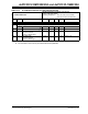
TABLE 24-9: DC CHARACTERISTICS: I/O PIN INPUT SPECIFICATIONS
DC CHARACTERISTICS
Standard Operating Conditions: 3.0V to 3.6V
(unless otherwise stated)
Operating temperature -40°C ≤ TA ≤ +85°C for Industrial
-40°C ≤ TA ≤+125°C for Extended
Param
No.
Symbol Characteristic Min Typ
(1)
Max Units Conditions
V
IL Input Low Voltage
DI10 I/O pins V
SS —0.2VDD V
DI15 MCLR
VSS —0.2VDD V
DI16 I/O Pins with OSC1 or SOSCI V
SS —0.2VDD V
DI18 SDAx, SCLx VSS — 0.3 VDD V SMBus disabled
DI19 SDAx, SCLx V
SS — 0.8 V V SMBus enabled
V
IH Input High Voltage
DI20 I/O Pins Not 5V Tolerant
(4)
I/O Pins 5V Tolerant
(4)
0.7 VDD
0.7 VDD
—
—
VDD
5.5
V
V
DI28 SDAx, SCLx 0.7 V
DD — 5.5 V SMBus disabled
DI29 SDAx, SCLx 2.1 — 5.5 V SMBus enabled
I
CNPU CNx Pull-up Current
DI30 50 250 400 μAV
DD = 3.3V, VPIN = VSS
Note 1: Data in “Typ” column is at 3.3V, 25°C unless otherwise stated.
2: The leakage current on the MCLR pin is strongly dependent on the applied voltage level. The specified
levels represent normal operating conditions. Higher leakage current may be measured at different input
voltages.
3: Negative current is defined as current sourced by the pin.
4: See “Pin Diagrams” for a list of digital-only and analog pins.
5: V
IL source < (VSS – 0.3). Characterized but not tested.
6: Non-5V tolerant pins V
IH source > (VDD + 0.3), 5V tolerant pins VIH source > 5.5V. Characterized but not
tested.
7: Digital 5V tolerant pins cannot tolerate any “positive” input injection current from input sources > 5.5V.
8: Injection currents > | 0 | can affect the ADC results by approximately 4-6 counts.
9: Any number and/or combination of I/O pins not excluded under I
ICL or IICH conditions are permitted pro-
vided the mathematical “absolute instantaneous” sum of the input injection currents from all pins do not
exceed the specified limit. Characterized but not tested.