
Information


2009-2013 Microchip Technology Inc. DS80000439N-page 5
dsPIC33FJ06GS101/X02 and dsPIC33FJ16GSX02/X04
Silicon Errata Issues
1. Module: PWM
Reading LEBCONx registers, as well as writing
individual bits and bytes within these registers
does not work.
Work around
Use a Word write operation to modify LEBCONx
registers. For example, to set the PHR bit within
the LEBCON1 register, use the following C code:
LEBCON1 = 0x8000
There is no work around for reading LEBCONx
registers.
Affected Silicon Revisions
2. Module: PWM
If PWM Immediate Update mode is selected
(IUE = 1), and the PWM duty cycle is provided via
the Master Duty Cycle (MDC) register (MDCS = 1
mode), the updates to the MDC register are
synchronized to the PWM time base instead of an
immediate update (duty cycle will be updated on
the next PWM period).
Work arounds
Work around 1:
Use the Enable Immediate Period Update mode
(EIPU = 1) in conjunction with PWM Immediate
Update mode (IUE = 1). This will update the period
and duty cycle on an immediate basis.
Work around 2:
Use individual duty cycle registers (PDCx) and
PWM Immediate Update mode (IUE = 1) to update
individual duty cycle registers on an immediate
basis.
Affected Silicon Revisions
3. Module: PWM
If PWM Fault interrupts are disabled (FLTIEN = 0
or CLIEN = 0), then associated Status bits
(FLTSTAT and CLSTAT) will not function.
Work around
Enable PWM Fault interrupts (FLTIEN = 1,
CLIEN = 1).
Affected Silicon Revisions
4. Module: PWM
The PWM output will exhibit jitter under the
following conditions:
When the PWM clock divider has the value of 1, 5
or 6 (PTCON2<PCLKDIV> = 0b001, 0b101 or
0b110), and the three Least Significant bits of the
PWM Period Register (PTPER or PHASEx), Duty
Cycle Register (MDC or PDCx) or Phase Register
(PHASEx) are non-zero.
Work around
Use PWM clock dividers other than 1, 5 or 6.
Affected Silicon Revisions
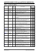
Note: This document summarizes all silicon
errata issues from all revisions of silicon,
previous as well as current. Only the
issues indicated by the shaded column in
the following tables apply to the current
silicon revision (A4).
A2 A3 A4
XX
X
A2 A3
A4
XX
X
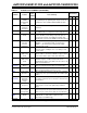
A2 A3 A4
XX
X
A2 A3
A4
XX
X