
Information


dsPIC33FJ06GS101/X02 and dsPIC33FJ16GSX02/X04
DS80000439N-page 4 2009-2013 Microchip Technology Inc.
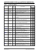
PWM Duty Cycle
Updates
34. When the PWM duty cycle update coincides with the PWM
period rollover, the PWM output may be corrupted for one
PWM period.
XXX
JTAG Active Pull-up 35. In JTAG mode, the TMS pin will not have an active pull-up
as required by the JTAG specification.
XXX
SPI Framed
Master Mode
36. When the SPI module is configured in Framed Master
mode and the Frame Sync Pulse Edge Select bit
(FRMDLY) is set to ‘1’, transmitting a word and then
buffering another word in the SPIxBUF register before the
transmission has completed, results in an incomplete
transmission of the first data word.
XXX
Comparator Trigger
Voltage Level
37. Output signal transitions occurring on the DACOUT pin
(with DAC output disabled) can cause the Comparator
trigger voltage level to change.
XXX
CPU Interrupt
Disable
38. When a previous DISI instruction is active (i.e., the
DISICNT register is non-zero), and the value of the
DISICNT register is updated manually, the DISICNT
register freezes and disables interrupts permanently.
XXX
CPU div.sd 39. When using the div.sd instruction, the overflow bit is not
getting set when an overflow occurs.
XXX
UART TX Interrupt 40. A Transmit (TX) interrupt may occur before the data
transmission is complete.
XXX
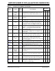
JTAG Flash
Programming
41. JTAG Flash programming is not supported. X X X
PWM PWM Module
Enable
42. If the PWM Clock Divider Select register, PTCON2, is not
equal to zero, the PWM module may or may not initialize
from an override state
XXX
PWM PWM SWAP 43. If the PWM is configured for Complimentary mode and the
SWAP bit is enabled, the PWM outputs might operate as
Redundant mode when the PHASE value is greater than
the programmed dead-time (DTRx) value.
XXX
PWM Current-Limit
Mode
44. A < 8-ns glitch may be observed on the PWM output pins
when the Current-Limit event occurs.
XXX
PWM Immediate
Update
45. Dead time is not asserted when PDCx is updated to cause
an immediate transition on the PWMxH and PWMxL
outputs.
XXX
ADC — 46. ADC measurement of INTREF may be zero under certain
start-up conditions.
XXX
TABLE 2: SILICON ISSUE SUMMARY (CONTINUED)
Module Feature
Item
Number
Issue Summary
Affected
Revisions
(1)
A2 A3 A4
Note 1: Only those issues indicated in the last column apply to the current silicon revision.