
Information


dsPIC33FJ06GS101/X02 and dsPIC33FJ16GSX02/X04
DS80000439N-page 2 2009-2013 Microchip Technology Inc.
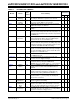
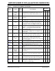
TABLE 2: SILICON ISSUE SUMMARY
Module Feature
Item
Number
Issue Summary
Affected
Revisions
(1)
A2 A3 A4
PWM Leading-Edge
Blanking
1. Reading LEBCONx registers, as well as writing individual
bits and bytes within these registers, does not work.
XXX
PWM Immediate
Updates
2. PWM Immediate Update mode (IEU = 1) for the Master
Duty Cycle register (MDC) is not functional.
XXX
PWM Status Bits 3. PWM Fault Status bits do not function if the associated
PWM Fault interrupts are disabled.
XXX
PWM Clock 4. PWM output will exhibit jitter with some PWM clock divider
settings.
XXX
PWM Faults 5. If the PWM is in Complementary, Redundant and Push-
Pull mode and the Independent Time Base bit (ITB) is set,
the Independent Fault mode may not work as expected for
the PWMxL pin.
XXX
PWM Independent
Time Base
6. The Independent Time Base PWM outputs may not be
synchronized with the Master time base PWM outputs
when both modes are used simultaneously.
XXX
PWM Latched Faults 7. In PWM Latched Fault mode, the PWM outputs may be
latched on both the rising as well as the falling edge of the
Fault signal regardless of the Fault input polarity selection
(set with the FCLCONx<FLTPOL> bit setting).
XXX
PWM Faults 8. A bit write to the CLMOD bit (bit 8) in the FCLCONx
register, or consecutive writes to the lower byte and higher
byte of the FCLCONx register, causes all other bits of the
high byte to be loaded with zeros.
XXX
PWM Sleep Mode 9. The PWM module fails to wake the CPU from Sleep mode
on a PWM Fault event.
XXX
Comparator — 10. For slow input signals, the Comparator module may
generate erroneous triggers/interrupts.
XXX
ADC Clock 11. Selecting the primary FRC (F
VCO) as a clock source for
the ADC module by setting the SLOWCLK bit
(ADCON<12>) to the default setting of ‘0’, does not work.
XXX
Auxiliary
Clock
Module
Disable
12. When the PWMMD bit in the PMD1 register is set, the
Auxiliary Clock to both the ADC and PWM modules is
disabled.
XXX
Comparator Interrupts 13. Comparator interrupts are incorrectly generated when the
High-Speed Analog Comparator is configured for an
inverted polarity setting (CMPCONx<CMPPOL> = 1).
XXX
UART 4x Mode 14. When the UART is in 4x mode (BRGH = 1) and using two
Stop bits (STSEL = 1), it may sample the first Stop bit
instead of the second one.
XXX
UART IR Interface
Operations
15. The 16x baud clock signal on the BCLK pin is present only
when the module is transmitting.
XXX
I
2
C™ 10-Bit
Addressing
Mode
16. When the I
2
C™ module is configured for 10-bit addressing
using the same address bits (A10 and A9) as other I
2
C
devices, the A10 and A9 bits may not work as expected.
XXX
PWM ADC
Conversion
17. The PWM module may fail to trigger a conversion on
certain ADC pairs when the primary or secondary PWMx
generator is selected as a trigger source.
X
Note 1: Only those issues indicated in the last column apply to the current silicon revision.