
Information


2009-2013 Microchip Technology Inc. DS80000439N-page 17
dsPIC33FJ06GS101/X02 and dsPIC33FJ16GSX02/X04
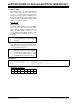
FIGURE 1: TIMING DIAGRAMS FOR CENTER-ALIGNED AND EDGE-ALIGNED MODES
46. Module: ADC
Depending on device start-up conditions,
measuring the internal voltage reference
(INTREF) with the ADC may return a value of 0V
in the result buffer.
Work around
None.
Affected Silicon Revisions
Center-Aligned Mode
Edge-Aligned Mode
PWMxL
PWMxH
PWMxL
PWMxH
PWMxL
PWMxH
PTMRx
Period
Period
PTMRx
0
PHASEx
PWMxH
PWMxH
PWMxH
PDC
OLD
PDCNEW > PDCOLD
PDCNEW < PDCOLD
PWMxL
PDC
NEW < PDCOLD
PDCNEW > PDCOLD
PDCOLD
0
PHASEx
PWMxL
PWMxL
A2 A3 A4
XX
X