
Information


dsPIC33FJ06GS101/X02 and dsPIC33FJ16GSX02/X04
DS80000439N-page 14 2009-2013 Microchip Technology Inc.
33. Module: Reserved
The issue in a previous version of the document
was removed.
34. Module: PWM
The High-Speed PWM provides a feature to
update the PWM duty cycle at any time during the
PWM period. The new duty cycle should take
effect:
• On the next PWM period when immediate duty
cycle updates are disabled
(PWMCONx<IUE> = 0).
• On the same PWM period when immediate
duty cycle updates are enabled
(PWMCONx<IUE> = 1).
However, when the immediate duty cycle updates
are disabled and the duty cycle update coincides
with a PWM period roll-over, the PWM output may
be corrupted and exhibit a 100% duty cycle for one
PWM period. The new duty cycle value will take
effect on the next PWM period.
Work around
Enable immediate duty cycle updates by
configuring PWMCONx<IUE> = 1.
Affected Silicon Revisions
35. Module: JTAG
In JTAG mode, the TMS pin will not have an active
pull-up as required by the JTAG specification.
Instead, the pull-up function will be enabled on the
TCK pin.
Work around
An external pull-up resistor can be connected to
the TMS pin to ensure that the signal does not
enter a tri-state condition when in JTAG mode.
There is no work around for the wrongly enabled
pull-up function on the TCK pin.
Affected Silicon Revisions
36. Module: SPI
When the SPI module is configured in Framed
Master mode and the Frame Sync Pulse Edge
Select bit (FRMDLY) is set to ‘1’, transmitting a
word and then buffering another word in the
SPIxBUF register before the transmission has
completed, results in an incomplete transmission
of the first data word. Only the first 15 bits from the
first data word are transmitted, followed by the
sync pulse and the complete second word.
Work around
Between the two back-to-back SPI operations,
add a delay to ensure that the first word is fully
transmitted before the second word is written to
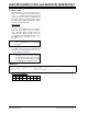
the SPIxBUF register, as shown in Example 4.
EXAMPLE 4:
Affected Silicon Revisions
37. Module: Comparator
With the DAC output is disabled by clearing the
DACOEN bit (CMPCONx<8>), output signal
transitions occurring on the DACOUT pin can
cause the comparator trigger voltage level to
change. For example, if the UART1 Transmit
(U1TX) signal is mapped to the same pin as
DACOUT, UART data transmissions can cause
the comparator to get triggered at different trigger
levels than what is programmed through the
CMPDACx register.
Work around
When the comparator is enabled, do not use the
DACOUT pin, either as a general purpose I/O pin
or a peripheral output signal.
Affected Silicon Revisions
A2 A3 A4
XX
X
Note: This issue is only present in the
dsPIC33FJ06GS101 device.
A2 A3
A4
XX
X
A2 A3 A4
XX
X
A2 A3 A4
XX
X
SPI1BUF = 0x0001;
while (SPI1STATbits.SPITBF);
asm ("REPEAT #50");.
asm ("NOP");
// The number of NOPs depends on the SPI
// clock prescalers
SPI1BUF = 0x0002;