
Information


2009-2013 Microchip Technology Inc. DS80000439N-page 13
dsPIC33FJ06GS101/X02 and dsPIC33FJ16GSX02/X04
32. Module: High-Speed PWM
The PENH and PENL bits in the IOCONx register
are used to assign ownership of the pins to either
the PWM module or the GPIO module. The correct
procedure to configure the PWM module is to
assign pin ownership to the PWM module and then
enabling it using the PTEN bit in the PTCON
register.
If the PWM module is enabled using the above
sequence, then a glitch may be observed on the
PWM pins before actual switching of the PWM
outputs begins. This glitch may cause momentary
turn-on of power MOSFETs that are driven by the
PWM pins and may cause damage to the
application hardware.
Work around
Follow the given sequence to avoid any glitches
from appearing on the PWM outputs at the time of
enabling.
1. Configure the respective PWM pins to digital
inputs using the TRISx registers. This step will
put the PWM pins in a high-impedance state.
The PWM outputs must be maintained in a safe
state by using pull-up or pull-down resistors.
2. Assign pin ownership to the GPIO module by
configuring IOCONx<PENH> = 0 and
IOCONx<PENL> = 0.
3. Specify the PWM override state to the desired
safe state for the PWM pins using the
OVRDAT<1:0> bit field in the IOCONx register.
4. Override the PWM outputs by
setting IOCONx<OVRENH> = 1 and
IOCONx<OVRENL> = 1.
5. Enable the PWM module by setting
PTCON<PTEN> = 1.
6. Remove the PWM overrides by
making IOCONx<OVRENH> = 0 and
IOCONx<OVRENL> = 0.
7. Ensure a delay of at least one full PWM cycle.
8. Assign pin ownership to the PWM module
by setting IOCONx<PENH> = 1 and
IOCONx<PENL> = 1.
The code in Example 3 illustrates the use of this
work around.
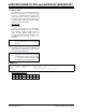
Affected Silicon Revisions
EXAMPLE 3: CONFIGURE PWM MODULE TO PREVENT GLITCHES ON PWM1H AND PWM1L
PINS AT THE TIME OF ENABLING
A2 A3 A4
XX
X
TRISAbits.TRISA4 = 1; // Configure PWM1H/RA4 as digital input
// Ensure output is in safe state using pull-up or
// pull-down resistors
TRISAbits.TRISA3 = 1; // Configure PWM1L/RA3 as digital input
// Ensure output is in safe state using pull-up or
// pull-down resistors
IOCON1bits.PENH = 0; // Assign pin ownership of PWM1H/RA4 to GPIO module
IOCON1bits.PENL = 0; // Assign pin ownership of PWM1L/RA3 to GPIO module
IOCON1bits.OVRDAT = 0; // Configure override state of the PWM outputs to
// desired safe state.
IOCON1bits.OVRENH = 1; // Override PWM1H output
IOCON1bits.OVRENL = 1; // Override PWM1L output
PTCONbits.PTEN = 1; // Enable PWM module
IOCON1bits.OVRENH = 0; // Remove override for PWM1H output
IOCON1bits.OVRENL = 0; // Remove override for PWM1L output
Delay(x); // Introduce a delay greater than one full PWM cycle
IOCON1bits.PENH = 1; // Assign pin ownership of PWM1H/RA4 to PWM module
IOCON1bits.PENL = 1; // Assign pin ownership of PWM1L/RA3 to PWM module