
Information

2010-2012 Microchip Technology Inc. DS80461G-page 5
dsPIC33FJ12MC201/202
7. Module: UART
When the UART is in 4x mode (BRGH = 1) and
using two Stop bits (STSEL = 1), it may sample the
first Stop bit instead of the second one.
This issue does not affect the other UART
configurations.
Work around
Use the 16x baud rate option (BRGH = 0) and
adjust the baud rate accordingly.
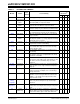
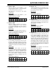
Affected Silicon Revisions
8. Module: UART
When the UART is configured for IR interface
operations (UxMODE<9:8> = 11), the 16x baud
clock signal on the BCLK pin is present only when
the module is transmitting. The pin is idle at all
other times.
Work around
Configure one of the output compare modules to
generate the required baud clock signal when the
UART is receiving data or in an Idle state.
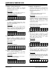
Affected Silicon Revisions
9. Module: Interrupt Controller
If a clock failure occurs when the device is in Idle
mode, the oscillator failure trap does not vector to
the Trap Service Routine. Instead, the device will
simply wake-up from Idle mode and continue code
execution if the Fail-Safe Clock Monitor (FSCM) is
enabled.
Work around
Whenever the device wakes up from Idle
(assuming the FSCM is enabled) the user software
should check the state of the OSCFAIL bit
(INTCON1<1>) to determine whether a clock
failure occurred, and then perform the appropriate
clock switch operation. Regardless, the Trap
Service Routine must be included in the user
application.
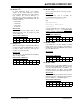
Affected Silicon Revisions
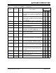
10. Module: SPI
Setting the DISSCK bit in the SPIxCON1 register
does not allow the user application to use the SCK
pin as a General Purpose I/O pin.
Work around
None.
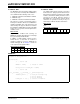
Affected Silicon Revisions
11. Module: I
2
C™
The BCL bit in I2CSTAT can be cleared only with a
16-bit operation, and can be corrupted with 1-bit or
8-bit operations on I2CSTAT.
Work around
Use 16-bit operations to clear BCL.
Affected Silicon Revisions
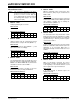
12. Module: I
2
C
If there are two I
2
C devices on the bus, one of
them is acting as the Master receiver and the other
as the Slave transmitter. If both devices are
configured for 10-bit addressing mode, and have
the same value in the A10 and A9 bits of their
addresses, then when the Slave select address is
sent from the Master, both the Master and Slave
acknowledge it. When the Master sends out the
read operation, both the Master and the Slave
enter into Read mode and both of them transmit
the data. The resultant data will be the ANDing of
the two transmissions.
Work around
In all I
2
C devices, the addresses as well as bits
A10 and A9 should be different.
Affected Silicon Revisions
A2 A3 A4 A5
XXX
X
A2 A3 A4 A5
XXX
X
A2 A3 A4
A5
XXX
X
A2 A3 A4 A5
XXX
X
A2 A3 A4 A5
XXX
X
A2 A3 A4 A5
XXX
X