
Information


dsPIC33F/PIC24H PROGRAMMING SPECIFICATION
DS70152H-page 64 © 2010 Microchip Technology Inc.
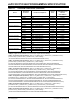
TABLE C-2: RESTORE DIAGNOSTIC AND CALIBRATION REGISTERS
Command (Binary) Data (Hex) Description
Step 1: Initialize TBLPAG and NVMCON to write stored diagnostic and Calibration Words.
0000 24001A MOV #0x4001, W10
0000 883B0A MOV W10, NVMCON
0000 200800 MOV #0x80, W0
0000 880190 MOV W0, TBLPAG
0000 207807 MOV #0x780, W7
0000 208006 MOV #0x800, W6
0000 000000 NOP
Step 2: Write stored diagnostic and Calibration Words.
0000 BB0BB6 TBLWTL[W6++], [W7]
0000 000000 NOP
0000 000000 NOP
0000 BBDBB6 TBLWTH.B[W6++], [W7++]
0000 000000 NOP
0000 000000 NOP
0000 BBEBB6 TBLWTH.B[W6++], [++W7]
0000 000000 NOP
0000 000000 NOP
0000 BB1BB6 TBLWTL[W6++], [W7++]
0000 000000 NOP
0000 000000 NOP
Step 3: Repeat step 2: thirty-two times.
Step 4: Initiate the write cycle.
0000 ABE761 BSET NVMCON, #WR
0000 000000 NOP
0000 000000 NOP
0000 000000 NOP
0000 000000 NOP
Step 5: Wait for Row Program operation to complete and make sure WR bit is clear.
— — Externally time ‘P13’ msec (see Section 8.0 “AC/DC
Characteristics and Timing Requirements”) to allow sufficient time
for the Row Program operation to complete.
0000 803B00 MOV NVMCON, W0
0000 883C20 MOV W0, VISI
0000 000000 NOP
0001 <VISI> Clock out contents of VISI register
0000 040200 GOTO 0x200
0000 000000 NOP
——Repeat until the WR bit is clear