
Information


dsPIC33F/PIC24H PROGRAMMING SPECIFICATION
DS70152H-page 60 © 2010 Microchip Technology Inc.
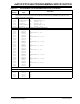
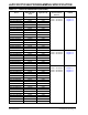
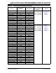
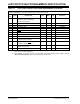
P9b TDLY5 Delay between PGDx ↓ by Programming
Executive to PGDx Released by
Programming Executive
15 23 μs—
P10 TDLY6 PGCx Low Time After Programming 400 — ns —
P11 TDLY7 Bulk Erase Time 330 — ms See Note 2
P12 T
DLY8 Page Erase Time 19.5 — ms See Note 2
P13 T
DLY9 Row Programming Time 1.28 — ms See Note 2
P14 T
R MCLR Rise Time to Enter ICSP mode — 1.0 μs—
P15 T
VALID Data Out Valid from PGCx ↑ 10 — ns —
P16 T
DLY10 Delay between Last PGCx ↓ and MCLR ↓ 0—s —
P17 T
HLD3MCLR ↓ to VDD ↓ —100ns —
P18 T
KEY1 Delay from First MCLR ↓ to First PGCx ↑
for Key Sequence on PGDx
1—μs—
P19 TKEY2 Delay from Last PGCx ↓ for Key Sequence
on PGDx to Second MCLR ↑
25 — ns —
P20 TDLY11 Maximum Wait Time for Configuration
Register Programming
—25ms —
P21 T
MCLRH MCLR High Time — 500 μs—
TABLE 8-1: AC/DC CHARACTERISTICS AND TIMING REQUIREMENTS (CONTINUED)
Standard Operating Conditions
Operating Temperature: –40ºC-85ºC. Programming at 25ºC is recommended.
Param
No.
Symbol Characteristic Min Max Units Conditions
Note 1: V
DD must also be supplied to the AVDD pins during programming. AVDD and AVSS should always be within
±0.3V of VDD and VSS, respectively.
2: Time depends on the FRC accuracy and the value of the FRC Oscillator tuning register. Refer to
“Electrical Characteristics” section in the specific device data sheet.