
Information


© 2010 Microchip Technology Inc. DS70152H-page 43
dsPIC33F/PIC24H PROGRAMMING SPECIFICATION
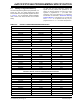
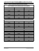
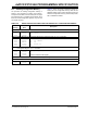
Table 5-7 shows the ICSP programming details for
clearing the Configuration registers. In Step 1, the
Reset vector is exited. In Step 2, the write pointer (W7)
is loaded with 0x0000, which is the original destination
address (in TBLPAG, 0xF8 of program memory). In
Step 3, the NVMCON is set to program one
Configuration register. In Step 4, the TBLPAG register
is initialized to 0xF8 for writing to the Configuration
registers. In Step 5, the value to write to each
Configuration register is loaded to W0. In Step 6, the
Configuration register data is written to the write latch
using the TBLWTL instruction. In Steps 7 and 8, the
programming cycle is initiated. In Step 9, the internal
PC is set to 0x200 as a safety measure to prevent the
PC from incrementing into unimplemented memory.
Lastly, Steps 4-9 are repeated until all twelve
Configuration registers are written.