
Information


© 2010 Microchip Technology Inc. DS70152H-page 41
dsPIC33F/PIC24H PROGRAMMING SPECIFICATION
5.7 Writing Configuration Memory
The 8-bit Configuration registers are programmable, one
register at a time. The default programming values
recommended for the Configuration registers are shown
in Table 5-6. The recommended default FOSCSEL
value is 0x00, which selects the FRC clock oscillator
setting.
The FBS, FSS and FGS Configuration registers are
special since they enable code protection for the
device. For security purposes, once any bit in these
registers is programmed to ‘0’ (to enable code
protection), it can only be set back to ‘1’ by performing
a Bulk Erase as described in Section 5.5 “Erasing
Program Memory”. Programming any of these bits
from a ‘0’ to ‘1’ is not possible, but they may be
programmed from a ‘1’ to ‘0’ to enable code protection.
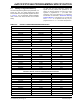
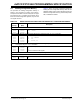
TABLE 5-6: DEFAULT CONFIGURATION REGISTER VALUES
dsPIC33FJ06GS101/102/202 AND dsPIC33FJ16GS402/404/502/504
Address Name Default Value
0xF80000 FBS 0x0F
0xF80004 FGS 0x07
0xF80006 FOSCSEL 0x87
0xF80008 FOSC 0xE7
0xF8000A FWDT 0xDF
0xF8000C FPOR 0x0F
0xF8000E FICD 0xE3
0xF80010 FUID0 0xFF
0xF80012 FUID1 0xFF
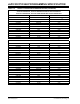
dsPIC33FJ12GP201/202, dsPIC33FJ12MC201/202 AND PIC24HJ12GP201/202
Address Name Default Value
0xF80000 FBS 0x0F
0xF80004 FGS 0x07
0xF80006 FOSCSEL 0x87
0xF80008 FOSC 0xE7
0xF8000A FWDT 0xDF
0xF8000C FPOR 0xF7
0xF8000E FICD 0xE3
0xF80010 FUID0 0xFF
0xF80012 FUID1 0xFF
0xF80014 FUID2 0xFF
0xF80016 FUID3 0xFF
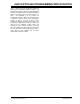
dsPIC33FJ32GP202/204, dsPIC33FJ32MC202/204 AND PIC24HJ32GP202/204
dsPIC33FJ16GP304, dsPIC33FJ16MC304 AND PIC24HJ16GP304
Address Name Default Value
0xF80000 FBS 0x0F
0xF80004 FGS 0x07
0xF80006 FOSCSEL 0x87
0xF80008 FOSC 0xE7
0xF8000A FWDT 0xDF
0xF8000C FPOR 0xF7
0xF8000E FICD 0xE3
0xF80010 FUID0 0xFF
0xF80012 FUID1 0xFF
0xF80014 FUID2 0xFF
0xF80016 FUID3 0xFF