
Information


dsPIC33F/PIC24H PROGRAMMING SPECIFICATION
DS70152H-page 40 © 2010 Microchip Technology Inc.
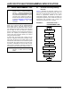
FIGURE 5-8: PROGRAM CODE MEMORY FLOW
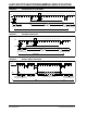
Step 8: Wait for Row Program operation to complete and make sure WR bit is clear.
—
0000
0000
0000
0001
0000
0000
—
—
803B00
883C20
000000
<VISI>
040200
000000
—
Externally time ‘P13’ msec (see Section 8.0 “AC/DC Characteristics and
Timing Requirements”) to allow sufficient time for the Row Program operation to
complete.
MOV NVMCON, W0
MOV W0, VISI
NOP
Clock out contents of VISI register.
GOTO 0x200
NOP
Repeat until the WR bit is clear.
Step 9: Repeat steps 3-8 until all code memory is programmed.
TABLE 5-5: SERIAL INSTRUCTION EXECUTION FOR WRITING CODE MEMORY (CONTINUED)
Command
(Binary)
Data
(Hex)
Description
Start Write Sequence
All
locations
done?
No
End
Start
Yes
Load 2 Bytes
to Write
Buffer at <Addr>
All
bytes
written?
No
Yes
and Poll for WR bit
to be cleared
N = 1
LoopCount = 0
Configure
Device for
Writes
N = 1
LoopCount =
LoopCount + 1
N = N + 1