
Information


© 2010 Microchip Technology Inc. DS70152H-page 33
dsPIC33F/PIC24H PROGRAMMING SPECIFICATION
5.2 Entering ICSP Mode
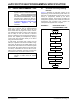
As illustrated in Figure 5-5, entering ICSP Program/
Verify mode requires three steps:
1. MCLR
is briefly driven high then low (P21)
(1)
.
2. A 32-bit key sequence is clocked into PGDx.
3. MCLR
is then driven high within a specified
period of time and held.
The programming voltage applied to MCLR
is VIH,
which is essentially V
DD in the case of dsPIC33F/
PIC24H devices. There is no minimum time require-
ment for holding at V
IH. After VIH is removed, an interval
of at least P18 must elapse before presenting the key
sequence on PGDx.
The key sequence is a specific 32-bit pattern,
‘0100 1101 0100 0011 0100 1000 0101 0001’
(more easily remembered as 0x4D434851 in
hexadecimal). The device will enter Program/Verify
mode only if the sequence is valid. The Most Significant
bit of the most significant nibble must be shifted in first.
Once the key sequence is complete, V
IH must be
applied to MCLR
and held at that level for as long as
Program/Verify mode is to be maintained. An interval of
at least time P19 and P7 must elapse before presenting
data on PGDx. Signals appearing on PGDx before P7
has elapsed will not be interpreted as valid.
On successful entry, the program memory can be
accessed and programmed in serial fashion. While in
ICSP mode, all unused I/Os are placed in the
high-impedance state.
5.3 ICSP Operation
After entering into ICSP mode, the CPU is Idle.
Execution of the CPU is governed by an internal state
machine. A 4-bit control code is clocked in using PGCx
and PGDx and this control code is used to command the
CPU (see Table 5- 1 ).
The SIX control code is used to send instructions to the
CPU for execution and the REGOUT control code is
used to read data out of the device via the VISI register.
TABLE 5-1: CPU CONTROL CODES IN
ICSP™ MODE
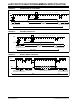
5.3.1 SIX SERIAL INSTRUCTION
EXECUTION
The SIX control code allows execution of dsPIC33F/
PIC24H Programming Specification assembly instruc-
tions. When the SIX code is received, the CPU is sus-
pended for 24 clock cycles, as the instruction is then
clocked into the internal buffer. Once the instruction is
shifted in, the state machine allows it to be executed over
the next four clock cycles. While the received instruction
is executed, the state machine simultaneously shifts in
the next 4-bit command (see Figure 5-3).
5.3.2 REGOUT SERIAL INSTRUCTION
EXECUTION
The REGOUT control code allows for data to be
extracted from the device in ICSP mode. It is used to
clock the contents of the VISI register out of the device
over the PGDx pin. After the REGOUT control code is
received, the CPU is held Idle for eight cycles. After these
eight cycles, an additional 16 cycles are required to clock
the data out (see Figure 5-4).
The REGOUT code is unique because the PGDx pin is
an input when the control code is transmitted to the
device. However, after the control code is processed,
the PGDx pin becomes an output as the VISI register is
shifted out.
Note 1: The MCLR
capacitor value can vary the
high time required for entering ICSP
mode.
4-Bit
Control Code
Mnemonic Description
0000b SIX Shift in 24-bit instruction
and execute.
0001b REGOUT Shift out the VISI
register.
0010b-1111b N/A Reserved.
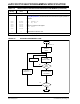
Note 1: Coming out of the ICSP entry sequence,
the first 4-bit control code is always
forced to SIX and a forced NOP instruction
is executed by the CPU. Five additional
PGCx clocks are needed on start-up,
thereby resulting in a 9-bit SIX command
instead of the normal 4-bit SIX command.
After the forced SIX is clocked in, ICSP
operation resumes as normal (the next
24 clock cycles load the first instruction
word to the CPU). See Figure 5-2 for
details.
2: TBLRDH, TBLRDL, TBLWTH and TBLWTL
instructions must be followed by a NOP
instruction.
Note: The device will latch input PGDx data on
the rising edge of PGCx and will output
data on the PGDx line on the rising edge
of PGCx. For all data transmissions, the
Least Significant bit (LSb) is transmitted
first.