
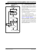
Information


© 2010 Microchip Technology Inc. DS70152H-page 15
dsPIC33F/PIC24H PROGRAMMING SPECIFICATION
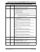
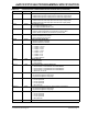
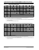
HPOL FPOR Motor Control PWM High-Side Polarity bit
1 = PWM module high-side output pins have active-high output polarity
0 = PWM module high-side output pins have active-low output polarity
LPOL FPOR Motor Control PWM Low-Side Polarity bit
1 = PWM module low-side output pins have active-high output polarity
0 = PWM module low-side output pins have active-low output polarity
ALTI2C FPOR Alternate I
2
C™ pins
1 = I
2
C mapped to SDA1/SCL1 pins
0 = I
2
C mapped to ASDA1/SACL1 pins
ALTQIO FPOR Enable Alternate QEI pins
1 = QEA1A, AEB1A and INDX1A are selected as inputs to QEI1
0 = QEA1, AEB1 and INDX1 are selected as inputs to QEI1
ALTSS1 FPOR Enable Alternate SS1 pins
1 = SS1A is selected as I/O to SPI1
0 = SS1 is selected as I/O to SPI1
BOREN FPOR Brown-out Reset Enable Bit
1 = BOR is enabled in hardware
0 = BOR is disabled in hardware
FPWRT<2:0> FPOR Power-on Reset Timer Value Select bits
111 = PWRT = 128 ms
110 = PWRT = 64 ms
101 = PWRT = 32 ms
100 = PWRT = 16 ms
011 = PWRT = 8 ms
010 = PWRT = 4 ms
001 = PWRT = 2 ms
000 = PWRT Disabled
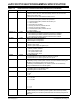
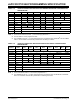
JTAGEN FICD JTAG Enable bit
1 = JTAG enabled
0 = JTAG disabled
ICS<1:0> FICD ICD Communication Channel Select bits
11 = Communicate on PGC1/EMUC1 and PGD1/EMUD1
10 = Communicate on PGC2/EMUC2 and PGD2/EMUD2
01 = Communicate on PGC3/EMUC3 and PGD3/EMUD3
00 = Reserved, do not use
CMPPOL0 FCMP Comparator Hysteresis Polarity (for even numbered comparators)
1 = Hysteresis is applied to falling edge
0 = Hysteresis is applied to rising edge
HYST0<1:0> FCMP Comparator Hysteresis Select
11 = 45 mV Hysteresis
10 = 30 mV Hysteresis
01 = 15 mV Hysteresis
00 = No Hysteresis
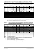
CMPPOL1 FCMP Comparator Hysteresis Polarity (for odd numbered comparators)
1 = Hysteresis is applied to falling edge
0 = Hysteresis is applied to rising edge
HYST1<1:0> FCMP Comparator Hysteresis Select
11 = 45 mV Hysteresis
10 = 30 mV Hysteresis
01 = 15 mV Hysteresis
00 = No Hysteresis
— All Unimplemented (read as ‘0’, write as ‘0’)
TABLE 3-2: dsPIC33F/PIC24H CONFIGURATION BITS DESCRIPTION (CONTINUED)
Bit Field Register Description