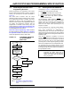
dsPIC33F/PIC24H dsPIC33F/PIC24H Flash Programming Specification 1.0 DEVICE OVERVIEW FIGURE 2-1: This document defines the programming specification for the dsPIC33F 16-bit Digital Signal Controller (DSC) and PIC24H 16-bit Microcontroller (MCU) families. This programming specification is required only for those developing programming support for the dsPIC33F/ PIC24H family. Customers using only one of these devices should use development tools that already provide support for device programming.
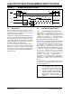
dsPIC33F/PIC24H PROGRAMMING SPECIFICATION FIGURE 2-2: 2.2 CONNECTIONS FOR THE ON-CHIP REGULATOR 3.3V The program Flash memory on the dsPIC33F/PIC24H has a specific write/erase requirement that must be adhered to, for proper device operation. The rule is that any given word in memory must not be written without first erasing the page in which it is located. Thus, the easiest way to conform to this rule is to write all the data in a programming block within one write cycle.
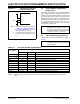
dsPIC33F/PIC24H PROGRAMMING SPECIFICATION 2.4 Memory Map The program memory map extends from 0x0 to 0xFFFFFE. Code storage is located at the base of the memory map and supports up to 88K instructions (about 256 Kbytes). Table 2-2 shows the program memory size and number of erase and program blocks present in each device variant. Each erase block or page contains 512 instructions and each program block or row, contains 64 instructions.
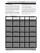
dsPIC33F/PIC24H PROGRAMMING SPECIFICATION TABLE 2-2: CODE MEMORY SIZE (CONTINUED) User Memory Address Limit (Instruction Words) Write Blocks Erase Blocks Executive Memory Address Limit (Instruction Words) dsPIC33FJ128GP710 0x0157FE (44K) 688 86 0x800FFE (2K) dsPIC33FJ128GP802 0x0157FE (44K) 688 86 0x800FFE (2K) dsPIC33F/PIC24H Device dsPIC33FJ128GP804 0x0157FE (44K) 688 86 0x800FFE (2K) dsPIC33FJ256GP506 0x02ABFE (88K) 1368 171 0x800FFE (2K) dsPIC33FJ256GP510 0x02ABFE (88K) 1368
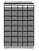
dsPIC33F/PIC24H PROGRAMMING SPECIFICATION TABLE 2-2: CODE MEMORY SIZE (CONTINUED) User Memory Address Limit (Instruction Words) Write Blocks Erase Blocks Executive Memory Address Limit (Instruction Words) PIC24HJ64GP210 0x00ABFE (22K) 344 43 0x800FFE (2K) PIC24HJ64GP502 0x00ABFE (22K) 344 43 0x800FFE (2K) PIC24HJ64GP504 0x00ABFE (22K) 344 43 0x800FFE (2K) PIC24HJ64GP506 0x00ABFE (22K) 344 43 0x800FFE (2K) PIC24HJ64GP510 0x00ABFE (22K) 344 43 0x800FFE (2K) PIC24HJ128GP202 0x015
dsPIC33F/PIC24H PROGRAMMING SPECIFICATION TABLE 2-2: CODE MEMORY SIZE (CONTINUED) User Memory Address Limit (Instruction Words) Write Blocks Erase Blocks dsPIC33FJ128MC710A 0x0157FE (44K) 688 86 0x800FFE (2k) PIC24HJ128GP206A 0x0157FE (44K) 688 86 0x800FFE (2k) PIC24HJ128GP210A 0x0157FE (44K) 688 86 0x800FFE (2k) PIC24HJ128GP306A 0x0157FE (44K) 688 86 0x800FFE (2k) PIC24HJ128GP310A 0x0157FE (44K) 688 86 0x800FFE (2k) PIC24HJ128GP506A 0x0157FE (44K) 688 86 0x800FFE (2k) dsPI
dsPIC33F/PIC24H PROGRAMMING SPECIFICATION FIGURE 2-3: PROGRAM MEMORY MAP 0x000000 User Flash Code Memory (87552 x 24-bit) User Memory Space 0x02ABFE 0x02AC00 Reserved 0x7FFFFE 0x800000 Executive Code Memory (2048 x 24-bit) 0x800FFE 0x801000 Configuration Memory Space Reserved Configuration Registers (12 x 8-bit) 0xF7FFFE 0xF80000 0xF80016 0xF80018 Reserved Device ID (2 x 16-bit) Reserved Note: 0xFEFFFE 0xFF0000 0xFF0002 0xFF0004 0xFFFFFE The address boundaries for user Flash and Executive cod
dsPIC33F/PIC24H PROGRAMMING SPECIFICATION 3.0 DEVICE PROGRAMMING – ENHANCED ICSP This section discusses programming the device through Enhanced ICSP and the programming executive. The programming executive resides in executive memory (separate from code memory) and is executed when Enhanced ICSP Programming mode is entered.
dsPIC33F/PIC24H PROGRAMMING SPECIFICATION 3.2 Confirming the Presence of the Programming Executive Before programming, the programmer must confirm that the programming executive is stored in executive memory. The procedure for this task is illustrated in Figure 3-2. First, ICSP mode is entered. Then, the unique Application ID Word stored in executive memory is read. If the programming executive is resident, the correct Application ID Word is read and programming can resume as normal.
dsPIC33F/PIC24H PROGRAMMING SPECIFICATION FIGURE 3-3: ENTERING ENHANCED ICSP™ MODE P6 P14 MCLR VDD P7 Program/Verify Entry Code = 0x4D434850 0 b31 PGDx 1 b30 0 b29 PGCx P18 3.4 P19 VIH VIH Blank Check The term “Blank Check” implies verifying that the device has been successfully erased and has no programmed memory locations. A blank or erased memory location is always read as ‘1’.
dsPIC33F/PIC24H PROGRAMMING SPECIFICATION FIGURE 3-4: FLOWCHART FOR PROGRAMMING CODE MEMORY Start PROGRAMMING VERIFICATION After code memory is programmed, the contents of memory can be verified to ensure that programming was successful. Verification requires code memory to be read back and compared against the copy held in the programmer’s buffer. The READP command can be used to read back all the programmed code memory.
dsPIC33F/PIC24H PROGRAMMING SPECIFICATION 3.6 Configuration Bits Programming 3.6.1 OVERVIEW The dsPIC33F/PIC24H devices have Configuration bits stored in twelve 8-bit Configuration registers, aligned on even configuration memory address boundaries. These bits can be set or cleared to select various device configurations. There are three types of Configuration bits: system operation bits, code-protect bits and unit ID bits.
dsPIC33F/PIC24H PROGRAMMING SPECIFICATION TABLE 3-2: Bit Field dsPIC33F/PIC24H CONFIGURATION BITS DESCRIPTION (CONTINUED) Register Description BWRP FBS Boot Segment Program Memory Write Protection 1 = Boot Segment program memory is not write-protected 0 = Boot Segment program memory is write-protected RSS<1:0> FSS Secure Segment Data RAM Code Protection 11 = No Data RAM is reserved for Secure Segment 10 = Small-Sized Secure RAM [(256 – N) bytes of RAM are reserved for Secure Segment in all other dev
dsPIC33F/PIC24H PROGRAMMING SPECIFICATION TABLE 3-2: Bit Field dsPIC33F/PIC24H CONFIGURATION BITS DESCRIPTION (CONTINUED) Register Description IESO FOSCSEL Two-Speed Oscillator Start-Up Enable bit 1 = Start-Up device with FRC, then automatically switch to the user-selected oscillator source when ready 0 = Start-Up device with user-selected oscillator source FNOSC<2:0> FOSCSEL Initial Oscillator Source Selection bits 111 = Internal Fast RC (FRC) oscillator with postscaler 110 = Internal Fast RC (FRC)
dsPIC33F/PIC24H PROGRAMMING SPECIFICATION TABLE 3-2: Bit Field dsPIC33F/PIC24H CONFIGURATION BITS DESCRIPTION (CONTINUED) Register Description HPOL FPOR Motor Control PWM High-Side Polarity bit 1 = PWM module high-side output pins have active-high output polarity 0 = PWM module high-side output pins have active-low output polarity LPOL FPOR Motor Control PWM Low-Side Polarity bit 1 = PWM module low-side output pins have active-high output polarity 0 = PWM module low-side output pins have active-low
dsPIC33F/PIC24H PROGRAMMING SPECIFICATION TABLE 3-3: Address dsPIC33FJ06GS101/X02 AND dsPIC33FJ16GSX02/X04 DEVICE CONFIGURATION REGISTER MAP Name Bit 7 Bit 6 Bit 5 Bit 4 0xF80000 FBS — — — — 0xF80002 Reserved — — — — — — — — — — — GSS<1:0> IESO — — — — — 0xF80004 FGS 0xF80006 FOSCSEL 0xF80008 FOSC FCKSM<1:0> Bit 3 IOL1WAY — FWDTEN WINDIS — WDTPRE 0xF8000C FPOR — — — — Reserved(2) JTAGEN(3) — — 0xF8000E FICD User Unit ID Byte 0 0xF80012 FUID1 User Unit ID Byt
dsPIC33F/PIC24H PROGRAMMING SPECIFICATION TABLE 3-5: Address dsPIC33FJ12MC201/202 DEVICE CONFIGURATION REGISTER MAP Name 0xF80000 FBS Bit 7 Bit 6 Bit 5 — — — 0xF80006 FOSCSEL Bit 3 — Bit 1 BSS<2:0> — — — IESO — — — — Bit 0 BWRP FCKSM<1:0> IOL1WAY — FWDTEN WINDIS — WDTPRE 0xF8000C FPOR PWMPIN LPOL ALTI2C — JTAGEN(2) — — HPOL GWRP FNOSC<2:0> 0xF8000A FWDT Reserved(1) GSS<1:0> — 0xF80008 FOSC 0xF8000E FICD Bit 2 Reserved(1) 0xF80002 Reserved 0xF80004 FGS Bit 4
dsPIC33F/PIC24H PROGRAMMING SPECIFICATION TABLE 3-7: Address dsPIC33FJ32MC202/204 AND dsPIC33FJ16MC304 DEVICE CONFIGURATION REGISTER MAP Name Bit 7 Bit 6 Bit 5 Bit 4 0xF80000 FBS — — — — 0xF80002 RESERVED — — — — — — — — IESO — — 0xF80004 FGS 0xF80006 FOSCSEL Bit 3 BSS<2:0> — GSS<1:0> — — — GWRP FNOSC<2:0> FCKSM<1:0> IOL1WAY — FWDTEN WINDIS — WDTPRE 0xF8000C FPOR PWMPIN LPOL ALTI2C — JTAGEN(2) — — HPOL Bit 0 BWRP — 0xF8000A FWDT Reserved(1) Bit 1 — 0xF8000
dsPIC33F/PIC24H PROGRAMMING SPECIFICATION TABLE 3-9: Address dsPIC33FJ32MC302/304, dsPIC33FJ64MCX02/X04 AND dsPIC33FJ128MCX02/X04 DEVICE CONFIGURATION REGISTER MAP Name Bit 7 Bit 6 Bit 5 Bit 4 Bit 3 Bit 2 Bit 1 Bit 0 0xF80000 FBS RBS<1:0> — — BSS<2:0> BWRP 0xF80002 FSS(1) RSS<1:0> — — SSS<2:0> SWRP — — — — IESO — — 0xF80004 FGS 0xF80006 FOSCSEL — FCKSM<1:0> IOL1WAY — 0xF8000A FWDT FWDTEN WINDIS — WDTPRE 0xF8000C FPOR PWMPIN LPOL ALTI2C — JTAGEN(3) — — HPOL Rese
dsPIC33F/PIC24H PROGRAMMING SPECIFICATION TABLE 3-11: dsPIC33FJXXXGPX06A/X08A/X10A AND PIC24HJXXXGPX06A/X08A/X10A DEVICE CONFIGURATION REGISTER MAP Address Name 0xF80000 0xF80002 0xF80004 0xF80006 FBS FSS FGS FOSCSEL Bit 7 Bit 6 RBS<1:0> RSS<1:0> — — IESO Reserved(2) 0xF80008 FOSC FCKSM<1:0> 0xF8000A FWDT FWDTEN WINDIS 0xF8000C FPOR Reserved(4) 0xF8000E FICD Reserved(1) 0xF80010 FUID0 0xF80012 FUID1 0xF80014 FUID2 0xF80016 FUID3 Legend: — = unimplemented bit, read as ‘0’.
dsPIC33F/PIC24H PROGRAMMING SPECIFICATION 3.6.2 PROGRAMMING METHODOLOGY Configuration bits may be programmed a single byte at a time using the PROGC command. This command specifies the configuration data and Configuration register address. Twelve PROGC commands are required to program all the Configuration bits. A flowchart for Configuration bit programming is illustrated in Figure 3-5.
dsPIC33F/PIC24H PROGRAMMING SPECIFICATION 3.6.4 CodeGuard™ SECURITY CONFIGURATION BITS The FBS, FSS and FGS Configuration registers are special Configuration registers that control the size and level of code protection for the Boot Segment, Secure Segment and General Segment, respectively. For each segment, two main forms of code protection are provided. One form prevents code memory from being written (write protection), while the other prevents code memory from being read (read protection).
dsPIC33F/PIC24H PROGRAMMING SPECIFICATION 4.0 THE PROGRAMMING EXECUTIVE Note: The Programming Executive (PE) can be located within the following folder within your installation of MPLAB® IDE: ...\Microchip\MPLAB IDE\REAL ICE, and then selecting the Hex PE file, RIPE_01b_xxxxxx.hex. 4.1 Programming Executive Communication The programmer and programming executive have a master-slave relationship, where the programmer is the master programming device and the programming executive is the slave.
dsPIC33F/PIC24H PROGRAMMING SPECIFICATION FIGURE 4-2: PROGRAMMING EXECUTIVE – PROGRAMMER COMMUNICATION PROTOCOL Host Transmits Last Command Word 1 2 Programming Executive Processes Command Host Clocks Out Response 1 15 16 2 15 16 1 2 15 16 PGCx PGDx MSB X X X LSB P8 PGCx = Input PGDx = Input Note 4.2 1: 0 P9a P9b PGCx = Input (Idle) PGDx = Output PGCx = Input PGDx = Output 4.2.2 The programming executive command set is shown in Table 4-1.
dsPIC33F/PIC24H PROGRAMMING SPECIFICATION TABLE 4-1: Opcode PROGRAMMING EXECUTIVE COMMAND SET Mnemonic Length (16-bit words) Time Out Description 0x0 SCHECK 1 1 ms Sanity check. 0x1 READC 3 1 ms Read an 8-bit word from the specified Configuration register or Device ID register. 0x2 READP 4 1 ms/row 0x3 Reserved N/A N/A This command is reserved. It will return a NACK. 0x4 PROGC 4 5 ms Write an 8-bit word to the specified Configuration register.
dsPIC33F/PIC24H PROGRAMMING SPECIFICATION 4.2.6 15 READC COMMAND 12 11 Opcode 4.2.7 8 7 0 15 12 11 8 7 Opcode Length N READP COMMAND 0 Length N Addr_MSB Reserved Addr_LS Addr_MSB Addr_LS Field Description Field Description Opcode 0x1 Length 0x3 Opcode N Number of 8-bit Configuration registers or Device ID registers to read (maximum of 256). Length 0x4 N Number of 24-bit instructions to read (maximum of 32768). Addr_MSB MSB of 24-bit source address.
dsPIC33F/PIC24H PROGRAMMING SPECIFICATION 4.2.8 PROGC COMMAND 15 12 11 4.2.9 8 7 Opcode 0 15 12 11 8 7 Opcode Length Reserved PROGP COMMAND 0 Length Reserved Addr_MSB Addr_MSB Addr_LS Addr_LS Data D_1 D_2 Field ... Description D_N Opcode 0x4 Length 0x4 Reserved 0x0 Addr_MSB MSB of 24-bit destination address. Opcode 0x5 Addr_LS Least Significant 16 bits of 24-bit destination address. Length 0x63 Reserved 0x0 8-bit data word.
dsPIC33F/PIC24H PROGRAMMING SPECIFICATION 4.2.10 ERASEP COMMAND 15 12 11 4.2.11 8 7 Opcode 0 Length 15 12 11 Opcode Addr_MSB NUM_PAGES CRCP COMMAND 8 7 Length Reserved Addr_MSB Addr_LSW Addr_LS Reserved Field Description Opcode 0x9 Length 0x3 NUM_PAGES Up to 255 Addr_MSB Addr_LS Most Significant Byte of the 24-bit address Least Significant 16 bits of the 24-bit address The ERASEP command instructs the programming executive to page erase [NUM_PAGES] of code memory.
dsPIC33F/PIC24H PROGRAMMING SPECIFICATION 4.2.12 QBLANK COMMAND 15 4.2.
dsPIC33F/PIC24H PROGRAMMING SPECIFICATION 4.3.1 RESPONSE FORMAT 4.3.1.2 All programming executive responses have a general format consisting of a two-word header and any required data for the command. 15 12 11 Opcode 8 7 Last_Cmd 0 QE_Code Length D_1 (if applicable) ... D_N (if applicable) Field Description Last_Cmd Field The Last_Cmd is a 4-bit field in the first word of the response and indicates the command that the programming executive processed.
dsPIC33F/PIC24H PROGRAMMING SPECIFICATION TABLE 4-4: QE_Code FOR NON-QUERY COMMANDS QE_Code Description 0x0 No error. 0x1 Verify failed. 0x2 Other error. 4.3.1.4 Response Length The response length indicates the length of the programming executive’s response in 16-bit words. This field includes the 2 words of the response header. With the exception of the response for the READP command, the length of each response is only 2 words.
dsPIC33F/PIC24H PROGRAMMING SPECIFICATION 5.0 Note: DEVICE PROGRAMMING – ICSP Any development tool that modifies the configuration memory on dsPIC33FJ06GS101/ 102/202, dsPIC33FJ16GS402/404/502/ 504, dsPIC33FJ32GS406/606/608/610 and dsPIC33FJ64GS406/606/608/610 devices must take care to preserve the data contained in the last six words of program memory. Refer to Appendix C: “Diagnostic and Calibration Registers” for more information.
dsPIC33F/PIC24H PROGRAMMING SPECIFICATION 5.2 Entering ICSP Mode 5.3.1 As illustrated in Figure 5-5, entering ICSP Program/ Verify mode requires three steps: MCLR is briefly driven high then low (P21)(1). A 32-bit key sequence is clocked into PGDx. MCLR is then driven high within a specified period of time and held. 1. 2. 3. Note 1: The MCLR capacitor value can vary the high time required for entering ICSP mode.
dsPIC33F/PIC24H PROGRAMMING SPECIFICATION FIGURE 5-2: PROGRAM ENTRY AFTER RESET P1 1 2 3 4 5 6 7 8 9 1 2 4 3 5 6 7 17 18 19 20 8 21 22 23 24 1 2 3 4 PGCx P4 P3 P1B P2 PGDx P4a P1A 0 0 0 0 0 0 0 0 LSB X 0 X X X X X Execute PC – 1, Fetch SIX Control Code X X X X X X X X MSB 0 24-bit Instruction Fetch 0 0 0 Execute 24-bit Instruction, Fetch Next Control Code PGDx = Input FIGURE 5-3: SIX SERIAL EXECUTION P1 1 3 2 4 1 2 3 4 5 6 7 17 18 19
dsPIC33F/PIC24H PROGRAMMING SPECIFICATION 5.4 Flash Memory Programming in ICSP Mode 5.4.1 TABLE 5-3: NVMCON Value PROGRAMMING OPERATIONS Flash memory write and erase operations are controlled by the NVMCON register. Programming is performed by setting NVMCON to select the type of erase operation (Table 5-2) or write operation (Table 5-3) and initiating the programming by setting the WR control bit (NVMCON<15>).
dsPIC33F/PIC24H PROGRAMMING SPECIFICATION REGISTER 5-1: NVMCON: FLASH MEMORY CONTROL REGISTER R/SO-0(1) R/W-0(1) R/W-0(1) U-0 U-0 U-0 U-0 U-0 WR WREN WRERR — — — — — bit 15 bit 8 R/W-0(1) U-0 — ERASE U-0 — R/W-0(1) U-0 R/W-0(1) R/W-0(1) R/W-0(1) NVMOP<3:0>(2) — bit 7 bit 0 Legend: SO = Satiable only bit R = Readable bit W = Writable bit U = Unimplemented bit, read as ‘0’ -n = Value at POR ‘1’ = Bit is set ‘0’ = Bit is cleared x = Bit is unknown bit 15 WR: Write Cont
dsPIC33F/PIC24H PROGRAMMING SPECIFICATION 5.5 Erasing Program Memory The procedure for erasing program memory (all of code memory, data memory, executive memory and code-protect bits) consists of setting NVMCON to 0x404F and then executing the programming cycle. For segment erase operations, the NVMCON value should be modified suitably, according to Table 5-2. Figure 5-6 illustrates the ICSP programming process for Bulk Erasing program memory.
dsPIC33F/PIC24H PROGRAMMING SPECIFICATION TABLE 5-4: Command (Binary) SERIAL INSTRUCTION EXECUTION FOR BULK ERASING CODE MEMORY Data (Hex) Description Step 1: Exit the Reset vector. 0000 0000 0000 040200 040200 000000 GOTO GOTO NOP 0x200 0x200 Step 2: Set the NVMCON to erase all program memory. 0000 0000 2404FA 883B0A MOV MOV #0x404F, W10 W10, NVMCON BSET NOP NOP NOP NOP NVMCON, #WR Step 3: Initiate the erase cycle.
dsPIC33F/PIC24H PROGRAMMING SPECIFICATION TABLE 5-5: Command (Binary) SERIAL INSTRUCTION EXECUTION FOR WRITING CODE MEMORY Data (Hex) Description Step 1: Exit the Reset vector. 0000 0000 0000 040200 040200 000000 GOTO GOTO NOP 0x200 0x200 Step 2: Set the NVMCON to program 64 instruction words. 0000 0000 24001A 883B0A MOV MOV #0x4001, W10 W10, NVMCON Step 3: Initialize the write pointer (W7) for TBLWT instruction.
dsPIC33F/PIC24H PROGRAMMING SPECIFICATION TABLE 5-5: Command (Binary) SERIAL INSTRUCTION EXECUTION FOR WRITING CODE MEMORY (CONTINUED) Data (Hex) Description Step 8: Wait for Row Program operation to complete and make sure WR bit is clear. — — 0000 0000 0000 0001 0000 0000 803B00 883C20 000000 040200 000000 — — Externally time ‘P13’ msec (see Section 8.0 “AC/DC Characteristics and Timing Requirements”) to allow sufficient time for the Row Program operation to complete.
dsPIC33F/PIC24H PROGRAMMING SPECIFICATION 5.7 Writing Configuration Memory The FBS, FSS and FGS Configuration registers are special since they enable code protection for the device. For security purposes, once any bit in these registers is programmed to ‘0’ (to enable code protection), it can only be set back to ‘1’ by performing a Bulk Erase as described in Section 5.5 “Erasing Program Memory”.
dsPIC33F/PIC24H PROGRAMMING SPECIFICATION TABLE 5-6: DEFAULT CONFIGURATION REGISTER VALUES (CONTINUED) dsPIC33FJ32GP302/304, dsPIC33FJ32MC302/304 AND PIC24HJ32GP302/304 dsPIC33FJ64GPX02/X04, dsPIC33FJ64MCX02/X04 AND PIC24HJ128GPX02/X04 dsPIC33FJ128GPX02/X04, dsPIC33FJ128MCX02/X04 AND PIC24HJ128GPX02/X04 Address Name Default Value 0xF80000 FBS 0x0F 0xF80002 FSS 0xCF/0xFF(1) 0xF80004 FGS 0x07 0xF80006 FOSCSEL 0x87 0xF80008 FOSC 0xE7 0xF8000A FWDT 0xDF 0xF8000C FPOR 0xF7 0xF8000E FICD 0xE3 0xF80010 FUID0 0
dsPIC33F/PIC24H PROGRAMMING SPECIFICATION Table 5-7 shows the ICSP programming details for clearing the Configuration registers. In Step 1, the Reset vector is exited. In Step 2, the write pointer (W7) is loaded with 0x0000, which is the original destination address (in TBLPAG, 0xF8 of program memory). In Step 3, the NVMCON is set to program one Configuration register. In Step 4, the TBLPAG register is initialized to 0xF8 for writing to the Configuration registers.
dsPIC33F/PIC24H PROGRAMMING SPECIFICATION TABLE 5-7: Command (Binary) SERIAL INSTRUCTION EXECUTION FOR WRITING CONFIGURATION REGISTERS Data (Hex) Description Step 1: Exit the Reset vector. 0000 0000 0000 040200 040200 000000 GOTO GOTO NOP 0x200 0x200 Step 2: Initialize the write pointer (W7) for the TBLWT instruction. 0000 200007 MOV #0x0000, W7 Step 3: Set the NVMCON register to program one Configuration register.
dsPIC33F/PIC24H PROGRAMMING SPECIFICATION 5.8 Reading Code Memory Reading from code memory is performed by executing a series of TBLRD instructions and clocking out the data using the REGOUT command. Table 5-8 shows the ICSP programming details for reading code memory. In Step 1, the Reset vector is exited. In Step 2, the 24-bit starting source address for reading is loaded into the TBLPAG register and W6 register.
dsPIC33F/PIC24H PROGRAMMING SPECIFICATION TABLE 5-8: Command (Binary) SERIAL INSTRUCTION EXECUTION FOR READING CODE MEMORY (CONTINUED) Data (Hex) Description Step 4: Output W0:W5 using the VISI register and REGOUT command.
dsPIC33F/PIC24H PROGRAMMING SPECIFICATION 5.9 Reading Configuration Memory The procedure for reading configuration memory is similar to the procedure for reading code memory, except that 16-bit data words are read (with the upper byte read being all ‘0’s) instead of 24-bit words. Since there are twelve Configuration registers, they are read one register at a time. TABLE 5-9: Command (Binary) Table 5-9 shows the ICSP programming details for reading all of the configuration memory.
dsPIC33F/PIC24H PROGRAMMING SPECIFICATION 5.10 Verify Code Memory and Configuration Word The verify step involves reading back the code memory space and comparing it against the copy held in the programmer’s buffer. The Configuration registers are verified with the rest of the code. The verify process is illustrated in Figure 5-9. Memory reads occur a single byte at a time, so two bytes must be read to compare against the word in the programmer’s buffer. Refer to Section 5.
dsPIC33F/PIC24H PROGRAMMING SPECIFICATION TABLE 5-10: Command (Binary) SERIAL INSTRUCTION EXECUTION FOR READING THE APPLICATION ID WORD Data (Hex) Description Step 1: Exit the Reset vector. 0000 0000 0000 040200 040200 000000 GOTO GOTO NOP 0x200 0x200 Step 2: Initialize TBLPAG and the read pointer (W0) for TBLRD instruction.
dsPIC33F/PIC24H PROGRAMMING SPECIFICATION 6.0 PROGRAMMING THE PROGRAMMING EXECUTIVE TO MEMORY 6.1 Overview Storing the programming executive to executive memory is similar to normal programming of code memory. Namely, the executive memory must first be erased, and then the programming executive must be programmed 64 words at a time. This control flow is summarized in Table 6-1. If it is determined that the programming executive is not present in executive memory (as described in Section 3.
dsPIC33F/PIC24H PROGRAMMING SPECIFICATION TABLE 6-1: Command (Binary) PROGRAMMING THE PROGRAMMING EXECUTIVE (CONTINUED) Data (Hex) Description Step 7: Load W0:W5 with the next 4 words of packed programming executive code and initialize W6 for programming. Programming starts from the base of executive memory (0x800000) using W6 as a read pointer and W7 as a write pointer.
dsPIC33F/PIC24H PROGRAMMING SPECIFICATION TABLE 6-1: Command (Binary) PROGRAMMING THE PROGRAMMING EXECUTIVE (CONTINUED) Data (Hex) Description Step 11: Wait for the Row Program operation to complete. — — 0000 0000 0000 0001 0000 0000 803B00 883C20 000000 040200 000000 — — Externally time ‘P13’ msec (see Section 8.0 “AC/DC Characteristics and Timing Requirements”) to allow sufficient time for the Row Program operation to complete.
dsPIC33F/PIC24H PROGRAMMING SPECIFICATION 6.2 Programming Verification After the programming executive has been programmed to executive memory using ICSP, it must be verified. Verification is performed by reading out the contents of executive memory and comparing it with the image of the programming executive stored in the programmer. TABLE 6-2: Command (Binary) Reading the contents of executive memory can be performed using the same technique described in Section 5.8 “Reading Code Memory”.
dsPIC33F/PIC24H PROGRAMMING SPECIFICATION TABLE 6-2: Command (Binary) READING EXECUTIVE MEMORY (CONTINUED) Data (Hex) Description Step 4: Output W0:W5 using the VISI register and REGOUT command.
dsPIC33F/PIC24H PROGRAMMING SPECIFICATION 7.0 DEVICE ID Table 7-1 lists the identification information for each device. The device ID region of memory can be used to determine mask, variant and manufacturing information about the chip. The device ID region is 2 x 16 bits and it can be read using the READC command. This region of memory is read-only and can also be read when code protection is enabled. TABLE 7-1: Table 7-2 shows the Device ID registers.
dsPIC33F/PIC24H PROGRAMMING SPECIFICATION TABLE 7-1: DEVICE IDs AND REVISION (CONTINUED) DEVID Register Value Application ID dsPIC33FJ128GP206 dsPIC33FJ128GP306 dsPIC33FJ128GP310 dsPIC33FJ128GP706 dsPIC33FJ128GP708 dsPIC33FJ128GP710 dsPIC33FJ128MC506 dsPIC33FJ128MC510 dsPIC33FJ128MC706 dsPIC33FJ128MC708 dsPIC33FJ128MC710 PIC24HJ128GP206 PIC24HJ128GP210 PIC24HJ128GP306 PIC24HJ128GP310 PIC24HJ128GP506 PIC24HJ128GP510 dsPIC33FJ256GP506 dsPIC33FJ256GP510 dsPIC33FJ256GP710 dsPIC33FJ256MC510 0x00D9 0x00E5 0x0
dsPIC33F/PIC24H PROGRAMMING SPECIFICATION TABLE 7-1: DEVICE IDs AND REVISION (CONTINUED) DEVID Register Value Application ID dsPIC33FJ128MC804 PIC24HJ32GP302 PIC24HJ32GP304 PIC24HJ64GP202 PIC24HJ64GP204 PIC24HJ64GP502 PIC24HJ64GP504 PIC24HJ128GP202 PIC24HJ128GP204 PIC24HJ128GP502 PIC24HJ128GP504 dsPIC33FJ64GP206A dsPIC33FJ64GP306A dsPIC33FJ64GP310A dsPIC33FJ64GP706A dsPIC33FJ64GP708A dsPIC33FJ64GP710A dsPIC33FJ64MC506A dsPIC33FJ64MC508A dsPIC33FJ64MC510A dsPIC33FJ64MC706A 0x062B 0x0645 0x0647 0x0655 0x0
dsPIC33F/PIC24H PROGRAMMING SPECIFICATION TABLE 7-1: DEVICE IDs AND REVISION (CONTINUED) Device DEVID Register Value Application ID dsPIC33FJ256GP506A dsPIC33FJ256GP510A dsPIC33FJ256GP710A dsPIC33FJ256MC510A dsPIC33FJ256MC710A PIC24HJ256GP206A PIC24HJ256GP210A PIC24HJ256GP610A dsPIC33FJ32GS406 dsPIC33FJ64GS406 dsPIC33FJ32GS606 dsPIC33FJ64GS606 dsPIC33FJ32GS608 dsPIC33FJ64GS608 dsPIC33FJ32GS610 dsPIC33FJ64GS610 0x07F5 0x07F7 0x07FF 0x07B7 0x07BF 0x0771 0x0773 0x077B 0x4000 0x4001 0x4002 0x4003 0x4004 0
dsPIC33F/PIC24H PROGRAMMING SPECIFICATION 8.0 AC/DC CHARACTERISTICS AND TIMING REQUIREMENTS Table 8-1 lists the AC/DC characteristics and timing requirements. TABLE 8-1: AC/DC CHARACTERISTICS AND TIMING REQUIREMENTS Standard Operating Conditions Operating Temperature: –40ºC-85ºC. Programming at 25ºC is recommended. Param Symbol No. D111 Characteristic VDD Supply Voltage During Programming Min Max Units 3.0 3.
dsPIC33F/PIC24H PROGRAMMING SPECIFICATION TABLE 8-1: AC/DC CHARACTERISTICS AND TIMING REQUIREMENTS (CONTINUED) Standard Operating Conditions Operating Temperature: –40ºC-85ºC. Programming at 25ºC is recommended. Param Symbol No.
dsPIC33F/PIC24H PROGRAMMING SPECIFICATION APPENDIX A: HEX FILE FORMAT Flash programmers process the standard HEX format used by the Microchip development tools. The format supported is the Intel® HEX32 Format (INHX32). Please refer to Appendix A in the “MPASM™ User’s Guide” (DS33014) for more information about hex file formats. The basic format of the hex file is: :BBAAAATTHHHH...HHHHCC Each data record begins with a 9-character prefix and always ends with a 2-character checksum.
dsPIC33F/PIC24H PROGRAMMING SPECIFICATION APPENDIX B: DEVICE ID REGISTER SILICON ERRATA ADDENDUM This silicon errata issue was previously published in the following documents, which are available from the Microchip web site: • dsPIC33FJXXXGPX06/X08/X10 Rev. A2 Silicon Errata (DS80306) • dsPIC33FJXXXMCX06/X08/X10 Rev. A2 Silicon Errata (DS80307) • PIC24HJXXXGPX06/X08/X10 Rev. A2 Silicon Errata (DS80280) This issue is included in this document to further assist customers. 1.
dsPIC33F/PIC24H PROGRAMMING SPECIFICATION APPENDIX C: DIAGNOSTIC AND CALIBRATION REGISTERS Table C-1 provides an example of how the diagnostic and calibration registers are read. This table can be added to the programming executive between steps 1 and 2. For dsPIC33FJ06GS101/102/202, dsPIC33FJ16GS402/ 404/502/504, dsPIC33FJ32GS406/606/608/610 and dsPIC33FJ64GS406/606/608/610 devices, the last six instruction words of program memory store diagnostic and calibration information.
dsPIC33F/PIC24H PROGRAMMING SPECIFICATION TABLE C-2: RESTORE DIAGNOSTIC AND CALIBRATION REGISTERS Command (Binary) Data (Hex) Description Step 1: Initialize TBLPAG and NVMCON to write stored diagnostic and Calibration Words. 0000 24001A MOV #0x4001, W10 0000 883B0A MOV W10, NVMCON 0000 200800 MOV #0x80, W0 0000 880190 MOV W0, TBLPAG 0000 207807 MOV #0x780, W7 0000 208006 MOV #0x800, W6 0000 000000 NOP Step 2: Write stored diagnostic and Calibration Words.
dsPIC33F/PIC24H PROGRAMMING SPECIFICATION APPENDIX D: TABLE D-1: CHECKSUM COMPUTATION CHECKSUM COMPUTATION Device dsPIC33FJ06GS101 dsPIC33FJ06GS102 dsPIC33FJ06GS202 dsPIC33FJ16GS402 dsPIC33FJ16GS404 dsPIC33FJ16GS502 dsPIC33FJ16GS504 dsPIC33FJ12GP201 dsPIC33FJ12GP202 dsPIC33FJ16GP304 Read Code Protection Disabled Enabled Disabled Enabled Disabled Enabled Disabled Enabled Disabled Enabled Disabled Enabled Disabled Enabled Disabled Enabled Disabled Enabled Disabled Enabled Checksum Computation CFGB + SUM(
dsPIC33F/PIC24H PROGRAMMING SPECIFICATION TABLE D-1: CHECKSUM COMPUTATION (CONTINUED) Device dsPIC33FJ32GP202 dsPIC33FJ32GP204 dsPIC33FJ32GP302 dsPIC33FJ32GP304 dsPIC33FJ64GP202 dsPIC33FJ64GP204 dsPIC33FJ64GP206 dsPIC33FJ64GP306 dsPIC33FJ64GP310 dsPIC33FJ64GP706 dsPIC33FJ64GP708 Read Code Protection Disabled Enabled Disabled Enabled Disabled Enabled Disabled Enabled Disabled Enabled Disabled Enabled Disabled Enabled Disabled Enabled Disabled Enabled Disabled Enabled Disabled Enabled Checksum Computation
dsPIC33F/PIC24H PROGRAMMING SPECIFICATION TABLE D-1: CHECKSUM COMPUTATION (CONTINUED) Device dsPIC33FJ64GP710 dsPIC33FJ64GP802 dsPIC33FJ64GP804 dsPIC33FJ128GP202 dsPIC33FJ128GP204 dsPIC33FJ128GP206 dsPIC33FJ128GP306 dsPIC33FJ128GP310 dsPIC33FJ128GP706 dsPIC33FJ128GP708 dsPIC33FJ128GP710 Read Code Protection Disabled Enabled Disabled Enabled Disabled Enabled Disabled Enabled Disabled Enabled Disabled Enabled Disabled Enabled Disabled Enabled Disabled Enabled Disabled Enabled Disabled Enabled Checksum Com
dsPIC33F/PIC24H PROGRAMMING SPECIFICATION TABLE D-1: CHECKSUM COMPUTATION (CONTINUED) Device dsPIC33FJ128GP802 dsPIC33FJ128GP804 dsPIC33FJ256GP506 dsPIC33FJ256GP510 dsPIC33FJ256GP710 dsPIC33FJ12MC201 dsPIC33FJ12MC202 dsPIC33FJ16MC304 dsPIC33FJ32MC202 dsPIC33FJ32MC204 dsPIC33FJ32MC302 Read Code Protection Disabled Enabled Disabled Enabled Disabled Enabled Disabled Enabled Disabled Enabled Disabled Enabled Disabled Enabled Disabled Enabled Disabled Enabled Disabled Enabled Disabled Enabled Checksum Comput
dsPIC33F/PIC24H PROGRAMMING SPECIFICATION TABLE D-1: CHECKSUM COMPUTATION (CONTINUED) Device dsPIC33FJ32MC304 dsPIC33FJ64MC202 dsPIC33FJ64MC204 dsPIC33FJ64MC506 dsPIC33FJ64MC508 dsPIC33FJ64MC510 dsPIC33FJ64MC706 dsPIC33FJ64MC710 dsPIC33FJ64MC802 dsPIC33FJ64MC804 dsPIC33FJ128MC202 Read Code Protection Disabled Enabled Disabled Enabled Disabled Enabled Disabled Enabled Disabled Enabled Disabled Enabled Disabled Enabled Disabled Enabled Disabled Enabled Disabled Enabled Disabled Enabled Checksum Computatio
dsPIC33F/PIC24H PROGRAMMING SPECIFICATION TABLE D-1: CHECKSUM COMPUTATION (CONTINUED) Device dsPIC33FJ128MC204 dsPIC33FJ128MC506 dsPIC33FJ128MC510 dsPIC33FJ128MC706 dsPIC33FJ128MC708 dsPIC33FJ128MC710 dsPIC33FJ256MC510 dsPIC33FJ256MC710 dsPIC33FJ128MC802 dsPIC33FJ128MC804 PIC24HJ12GP201 Read Code Protection Disabled Enabled Disabled Enabled Disabled Enabled Disabled Enabled Disabled Enabled Disabled Enabled Disabled Enabled Disabled Enabled Disabled Enabled Disabled Enabled Disabled Enabled Checksum Com
dsPIC33F/PIC24H PROGRAMMING SPECIFICATION TABLE D-1: CHECKSUM COMPUTATION (CONTINUED) Device PIC24HJ12GP202 PIC24HJ16GP304 PIC24HJ32GP202 PIC24HJ32GP204 PIC24HJ32GP302 PIC24HJ32GP304 PIC24HJ64GP202 PIC24HJ64GP204 PIC24HJ64GP206 PIC24HJ64GP210 PIC24HJ64GP502 Read Code Protection Disabled Enabled Disabled Enabled Disabled Enabled Disabled Enabled Disabled Enabled Disabled Enabled Disabled Enabled Disabled Enabled Disabled Enabled Disabled Enabled Disabled Enabled Checksum Computation CFGB + SUM(0:001FFF)
dsPIC33F/PIC24H PROGRAMMING SPECIFICATION TABLE D-1: CHECKSUM COMPUTATION (CONTINUED) Device PIC24HJ64GP504 PIC24HJ64GP506 PIC24HJ64GP510 PIC24HJ128GP202 PIC24HJ128GP204 PIC24HJ128GP206 PIC24HJ128GP210 PIC24HJ128GP306 PIC24HJ128GP310 PIC24HJ128GP502 Read Code Protection Disabled Enabled Disabled Enabled Disabled Enabled Disabled Enabled Disabled Enabled Disabled Enabled Disabled Enabled Disabled Enabled Disabled Enabled Disabled Enabled Checksum Computation CFGB + SUM(0:00ABFF) CFGB CFGB + SUM(0:00ABFF)
dsPIC33F/PIC24H PROGRAMMING SPECIFICATION TABLE D-1: CHECKSUM COMPUTATION (CONTINUED) Device PIC24HJ128GP504 PIC24HJ128GP506 PIC24HJ128GP510 PIC24HJ256GP206 PIC24HJ256GP210 PIC24HJ256GP610 dsPIC33FJ64GP206A dsPIC33FJ64GP306A dsPIC33FJ64GP310A dsPIC33FJ64GP706A dsPIC33FJ64GP708A Read Code Protection Disabled Enabled Disabled Enabled Disabled Enabled Disabled Enabled Disabled Enabled Disabled Enabled Disabled Enabled Disabled Enabled Disabled Enabled Disabled Enabled Disabled Enabled Checksum Computation
dsPIC33F/PIC24H PROGRAMMING SPECIFICATION TABLE D-1: CHECKSUM COMPUTATION (CONTINUED) Device dsPIC33FJ64GP710A dsPIC33FJ64MC506A dsPIC33FJ64MC508A dsPIC33FJ64MC510A dsPIC33FJ64MC706A dsPIC33FJ64MC710A PIC24HJ64GP206A PIC24HJ64GP210A PIC24HJ64GP506A PIC24HJ64GP510A dsPIC33FJ128GP206A Read Code Protection Disabled Enabled Disabled Enabled Disabled Enabled Disabled Enabled Disabled Enabled Disabled Enabled Disabled Enabled Disabled Enabled Disabled Enabled Disabled Enabled Disabled Enabled Checksum Computa
dsPIC33F/PIC24H PROGRAMMING SPECIFICATION TABLE D-1: CHECKSUM COMPUTATION (CONTINUED) Device dsPIC33FJ128GP306A dsPIC33FJ128GP310A dsPIC33FJ128GP706A dsPIC33FJ128GP708A dsPIC33FJ128GP710A dsPIC33FJ128MC506A dsPIC33FJ128MC510A dsPIC33FJ128MC706A dsPIC33FJ128MC708A dsPIC33FJ128MC710A PIC24HJ128GP206A Read Code Protection Disabled Enabled Disabled Enabled Disabled Enabled Disabled Enabled Disabled Enabled Disabled Enabled Disabled Enabled Disabled Enabled Disabled Enabled Disabled Enabled Disabled Enabled
dsPIC33F/PIC24H PROGRAMMING SPECIFICATION TABLE D-1: CHECKSUM COMPUTATION (CONTINUED) Device PIC24HJ128GP210A PIC24HJ128GP306A PIC24HJ128GP310A PIC24HJ128GP506A PIC24HJ128GP510A dsPIC33FJ256GP506A dsPIC33FJ256GP510A dsPIC33FJ256GP710A dsPIC33FJ256MC510A dsPIC33FJ256MC710A PIC24HJ256GP206A Read Code Protection Disabled Enabled Disabled Enabled Disabled Enabled Disabled Enabled Disabled Enabled Disabled Enabled Disabled Enabled Disabled Enabled Disabled Enabled Disabled Enabled Disabled Enabled Checksum C
dsPIC33F/PIC24H PROGRAMMING SPECIFICATION TABLE D-1: CHECKSUM COMPUTATION (CONTINUED) Device PIC24HJ256GP210A PIC24HJ256GP610A dsPIC33FJ32GS406 dsPIC33FJ64GS406 dsPIC33FJ32GS606 dsPIC33FJ64GS606 dsPIC33FJ32GS608 dsPIC33FJ64GS608 dsPIC33FJ32GS610 dsPIC33FJ64GS610 Read Code Protection Disabled Enabled Disabled Enabled Disabled Enabled Disabled Enabled Disabled Enabled Disabled Enabled Disabled Enabled Disabled Enabled Disabled Enabled Disabled Enabled Checksum Computation Erased Value Value with 0xAAAAA
dsPIC33F/PIC24H PROGRAMMING SPECIFICATION Table D-2 provides an example of how to calculate the checksum when using CodeGuard™ Security with Boot Segment Program Flash code protection with Standard Security and small-sized boot Flash.
dsPIC33F/PIC24H PROGRAMMING SPECIFICATION APPENDIX E: REVISION HISTORY Revision C (June 2006) • Added code protection Configuration register descriptions • Added information about Unit ID • Added ERASES, ERASEG and ERASEC programming executive commands • Added checksum computation equation Revision D (March 2007) • Added information specific to the dsPIC33FJ12GP201/202, dsPIC33FJ12MC201/ 202 and PIC24HJ12GP201/202 devices in several sections, including pinout diagrams, program memory sizes and Device ID
dsPIC33F/PIC24H PROGRAMMING SPECIFICATION Revision F (March 2008) Revision G (March 2009) • Removed Preliminary status from document footer • Added information specific to the following new devices in several sections, including program memory sizes, Configuration bit descriptions, checksum computations, Configuration registers and Device ID values: This revision includes minor updates to the text such as typographical errors, formatting and grammar.
dsPIC33F/PIC24H PROGRAMMING SPECIFICATION Revision G (March 2009) (Continued) • Removed PROGW and renamed QBLANK to QBLANKEX in the Command Set Summary, and added the following commands (see Table 3-1): - ERASEB - ERASEP - CRCP • Updated the flowchart in Figure 3-2 • Updated the second paragraph in Section 3.
dsPIC33F/PIC24H PROGRAMMING SPECIFICATION Revision H (October 2010) This revision includes the following updates: • Text and formatting updates have been incorporated throughout the document • All references to VCAP/VDDCORE have been changed to: VCAP • All occurrences of PGC and PGD have been changed to PGCx and PGDx, respectively • Added topics covered in Section 1.
Note the following details of the code protection feature on Microchip devices: • Microchip products meet the specification contained in their particular Microchip Data Sheet. • Microchip believes that its family of products is one of the most secure families of its kind on the market today, when used in the intended manner and under normal conditions. • There are dishonest and possibly illegal methods used to breach the code protection feature.
Worldwide Sales and Service AMERICAS ASIA/PACIFIC ASIA/PACIFIC EUROPE Corporate Office 2355 West Chandler Blvd. Chandler, AZ 85224-6199 Tel: 480-792-7200 Fax: 480-792-7277 Technical Support: http://support.microchip.com Web Address: www.microchip.