
Datasheet


© 2007-2012 Microchip Technology Inc. DS70292G-page 147
dsPIC33FJ32GP302/304, dsPIC33FJ64GPX02/X04, AND dsPIC33FJ128GPX02/X04
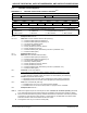
REGISTER 9-2: CLKDIV: CLOCK DIVISOR REGISTER
(2)
R/W-0 R/W-0 R/W-1 R/W-1 R/W-0 R/W-0 R/W-0 R/W-0
ROI DOZE<2:0> DOZEN
(1)
FRCDIV<2:0>
bit 15 bit 8
R/W-0 R/W-1 U-0 R/W-0 R/W-0 R/W-0 R/W-0 R/W-0
PLLPOST<1:0> — PLLPRE<4:0>
bit 7 bit 0
Legend: y = Value set from Configuration bits on POR
R = Readable bit W = Writable bit U = Unimplemented bit, read as ‘0’
-n = Value at POR ‘1’ = Bit is set ‘0’ = Bit is cleared x = Bit is unknown
bit 15 ROI: Recover on Interrupt bit
1 = Interrupts clears the DOZEN bit and the processor clock/peripheral clock ratio is set to 1:1
0 = Interrupts have no effect on the DOZEN bit
bit 14-12 DOZE<2:0>: Processor Clock Reduction Select bits
111 = F
CY/128
110 = FCY/64
101 = F
CY/32
100 = FCY/16
011 = FCY/8 (default)
010 = F
CY/4
001 = FCY/2
000 = FCY/1
bit 11 DOZEN: Doze Mode Enable bit
(1)
1 = DOZE<2:0> field specifies the ratio between the peripheral clocks and the processor clocks
0 = Processor clock/peripheral clock ratio forced to 1:1
bit 10-8 FRCDIV<2:0>: Internal Fast RC Oscillator Postscaler bits
111 = FRC divide by 256
110 = FRC divide by 64
101 = FRC divide by 32
100 = FRC divide by 16
011 = FRC divide by 8
010 = FRC divide by 4
001 = FRC divide by 2
000 = FRC divide by 1 (default)
bit 7-6 PLLPOST<1:0>: PLL VCO Output Divider Select bits (also denoted as ‘N2’, PLL postscaler)
11 = Output/8
10 = Reserved
01 = Output/4 (default)
00 = Output/2
bit 5 Unimplemented: Read as ‘0’
bit 4-0 PLLPRE<4:0>: PLL Phase Detector Input Divider bits (also denoted as ‘N1’, PLL prescaler)
11111 = Input/33
•
•
•
00000 = Input/2 (default)
00001 = Input/3
Note 1: This bit is cleared when the ROI bit is set and an interrupt occurs.
2: This register is reset only on a Power-on Reset (POR).