
Datasheet


© 2007-2012 Microchip Technology Inc. DS70292G-page 55
dsPIC33FJ32GP302/304, dsPIC33FJ64GPX02/X04, AND dsPIC33FJ128GPX02/X04
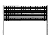
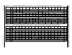
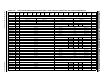
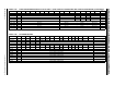
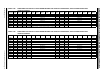
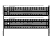
TABLE 4-21: PERIPHERAL PIN SELECT INPUT REGISTER MAP
File Name Addr Bit 15 Bit 14 Bit 13 Bit 12 Bit 11 Bit 10 Bit 9 Bit 8 Bit 7 Bit 6 Bit 5 Bit 4 Bit 3 Bit 2 Bit 1 Bit 0
All
Resets
RPINR0
0680
— — — INT1R<4:0> — — — — — — — —
1F00
RPINR1
0682
— — — — — — — — — — —INT2R<4:0>
001F
RPINR3
0686
— — —T3CKR<4:0>— — —T2CKR<4:0>
1F1F
RPINR4
0688
— — —T5CKR<4:0>— — —T4CKR<4:0>
1F1F
RPINR7
068E
— — — IC2R<4:0> — — — IC1R<4:0>
1F1F
RPINR10
0694
— — — IC8R<4:0> — — — IC7R<4:0>
1F1F
RPINR11
0696
— — — — — — — — — — —OCFAR<4:0>
001F
RPINR18
06A4
— — — U1CTSR<4:0> — — —U1RXR<4:0>
1F1F
RPINR19
06A6
— — — U2CTSR<4:0> — — —U2RXR<4:0>
1F1F
RPINR20
06A8
— — —SCK1R<4:0>— — —SDI1R<4:0>
1F1F
RPINR21
06AA
— — — — — — — — — — — SS1R<4:0>
001F
RPINR22
06AC
— — —SCK2R<4:0>— — —SDI2R<4:0>
1F1F
RPINR23
06AE
— — — — — — — — — — — SS2R<4:0>
001F
RPINR24
06B0
— — — CSCKR<4:0> — — —CSDIR<4:0>
1F1F
RPINR25
06B2
— — — — — — — — — — —COFSR<4:0>
001F
RPINR26
(1)
06B4 — — — — — — — — — — —C1RXR<4:0>
001F
Legend: x = unknown value on Reset, — = unimplemented, read as ‘0’. Reset values are shown in hexadecimal.
Note 1: This register is present only for dsPIC33FJ128GP802/804 and dsPIC33FJ64GP802/804