
Datasheet


© 2007-2012 Microchip Technology Inc. DS70292G-page 5
dsPIC33FJ32GP302/304, dsPIC33FJ64GPX02/X04, AND dsPIC33FJ128GPX02/X04
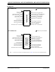
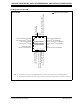
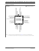
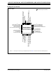
Pin Diagrams (Continued)
28-Pin QFN-S
(2)
dsPIC33FJ128GP202
MCLR
VSS
VDD
AN0/
V
REF
+/CN2/RA0
AN1/
V
REF
-/CN3/RA1
AV
DD
AVSS
PGED1/
AN2/C2IN-/RP0
(1)
/CN4/RB0
PGEC3/ASCL1/RP6
(1)
/CN24/PMD6/RB6
SOSCO/T1CK/CN0/PMA1/RA4
SOSCI/
RP4
(1)
/CN1/PMBE/RB4
VSS
OSC2/CLKO/CN29/PMA0/RA3
OSC1/CLKI/CN30/RA2
V
CAP
INT0/RP7
(1)
/CN23/PMD5/RB7
TDO/SDA1/RP9
(1)
/CN21/PMD3/RB9
TCK/SCL1/RP8
(1)
/CN22/PMD4/RB8
AN5/C1IN+/RP3
(1)
/CN7/RB3
AN4/C1IN-/
RP2
(1)
/CN6/RB2
PGEC1/
AN3/C2IN+/RP1
(1)
/CN5/RB1
AN9/DAC1LN/
RP15
(1)
/CN11/PMCS1/RB15
AN10/DAC1LP/RTCC/
RP14
(1)
/CN12/PMWR/RB14
AN11/
RP13
(1)
/CN13/PMRD/RB13
AN12/
RP12
(1)
/CN14/PMD0/RB12
PGED2/TDI/RP10
(1)
/CN16/PMD2/RB10
PGEC2/TMS/RP11
(1)
/CN15/PMD1/RB11
PGED3/ASDA1/RP5
(1)
/CN27/PMD7/RB5
dsPIC33FJ64GP202
dsPIC33FJ32GP302
Note 1: The RPx pins can be used by any remappable peripheral. See Tabl e 1 in this section for the list of available peripherals.
2: The metal plane at the bottom of the device is not connected to any pins and is recommended to be connected to VSS externally.
=
Pins are up to 5V tolerant
2
3
6
1
18
19
20
21
22
15
7
16
17
23
24
25
26
27
2
8
5
4
14
13
12
11
10
9
8