
Datasheet


dsPIC33FJ32GP302/304, dsPIC33FJ64GPX02/X04, AND dsPIC33FJ128GPX02/X04
DS70292G-page 48 © 2007-2012 Microchip Technology Inc.
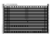
TABLE 4-10: UART2 REGISTER MAP
SFR Name
SFR
Addr
Bit 15 Bit 14 Bit 13 Bit 12 Bit 11 Bit 10 Bit 9 Bit 8 Bit 7 Bit 6 Bit 5 Bit 4 Bit 3 Bit 2 Bit 1 Bit 0
All
Resets
U2MODE 0230 UARTEN — USIDL IREN RTSMD — UEN1 UEN0 WAKE LPBACK ABAUD URXINV BRGH PDSEL<1:0> STSEL
0000
U2STA 0232 UTXISEL1 UTXINV UTXISEL0 — UTXBRK UTXEN UTXBF TRMT URXISEL<1:0> ADDEN RIDLE PERR FERR OERR URXDA
0110
U2TXREG 0234 — — — — — — — UTX8 UART Transmit Register
xxxx
U2RXREG 0236 — — — — — — — URX8 UART Receive Register
0000
U2BRG 0238 Baud Rate Generator Prescaler
0000
Legend: x = unknown value on Reset, — = unimplemented, read as ‘0’. Reset values are shown in hexadecimal.
TABLE 4-11: SPI1 REGISTER MAP
SFR Name
SFR
Addr
Bit 15 Bit 14 Bit 13 Bit 12 Bit 11 Bit 10 Bit 9 Bit 8 Bit 7 Bit 6 Bit 5 Bit 4 Bit 3 Bit 2 Bit 1 Bit 0
All
Resets
SPI1STAT 0240 SPIEN — SPISIDL — — — — — —SPIROV— — — — SPITBF SPIRBF
0000
SPI1CON1 0242 — — — DISSCK DISSDO MODE16 SMP CKE SSEN CKP MSTEN SPRE<2:0> PPRE<1:0>
0000
SPI1CON2 0244 FRMEN SPIFSD FRMPOL — — — — — — — — — — — FRMDLY —
0000
SPI1BUF 0248 SPI1 Transmit and Receive Buffer Register
0000
Legend: x = unknown value on Reset, — = unimplemented, read as ‘0’. Reset values are shown in hexadecimal.
TABLE 4-12: SPI2 REGISTER MAP
SFR Name
SFR
Addr
Bit 15 Bit 14 Bit 13 Bit 12 Bit 11 Bit 10 Bit 9 Bit 8 Bit 7 Bit 6 Bit 5 Bit 4 Bit 3 Bit 2 Bit 1 Bit 0
All
Resets
SPI2STAT 0260 SPIEN — SPISIDL — — — — — —SPIROV— — — — SPITBF SPIRBF
0000
SPI2CON1 0262 — — — DISSCK DISSDO MODE16 SMP CKE SSEN CKP MSTEN SPRE<2:0> PPRE<1:0>
0000
SPI2CON2 0264 FRMEN SPIFSD FRMPOL — — — — — — — — — — — FRMDLY —
0000
SPI2BUF 0268 SPI2 Transmit and Receive Buffer Register
0000
Legend: x = unknown value on Reset, — = unimplemented, read as ‘0’. Reset values are shown in hexadecimal.