
Datasheet


dsPIC33FJ32GP302/304, dsPIC33FJ64GPX02/X04, AND dsPIC33FJ128GPX02/X04
DS70292G-page 384 © 2007-2012 Microchip Technology Inc.
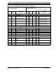
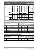
TABLE 30-44: ADC CONVERSION (12-BIT MODE) TIMING REQUIREMENTS
AC CHARACTERISTICS
Standard Operating Conditions: 3.0V to 3.6V
(unless otherwise stated)
Operating temperature -40°C ≤ TA ≤ +85°C for Industrial
-40°C ≤T
A ≤+125°C for Extended
Param
No.
Symbol Characteristic Min. Typ
(2)
Max. Units Conditions
Clock Parameters
(1)
AD50 TAD ADC Clock Period 117.6 — — ns —
AD51 t
RC ADC Internal RC Oscillator
Period
— 250 — ns —
Conversion Rate
AD55 t
CONV Conversion Time — 14 TAD ns —
AD56 F
CNV Throughput Rate — — 500 ksps —
AD57 TSAMP Sample Time 3 TAD —— — —
Timing Parameters
AD60 t
PCS
Conversion Start from Sample
Trigger
(2)
2 TAD —3 TAD — Auto convert trigger not
selected
AD61 t
PSS Sample Start from Setting
Sample (SAMP) bit
(2)
2 TAD —3 TAD ——
AD62 t
CSS Conversion Completion to
Sample Start (ASAM = 1)
(2)
— 0.5 TAD —— —
AD63 tDPU Time to Stabilize Analog Stage
from ADC Off to ADC On
(2,3)
——20μs—
Note 1: Because the sample caps eventually loses charge, clock rates below 10 kHz may affect linearity
performance, especially at elevated temperatures.
2: These parameters are characterized but not tested in manufacturing.
3: The t
DPU is the time required for the ADC module to stabilize at the appropriate level when the module is
turned on ADON bit (AD1CON1<15>) = ‘1’. During this time, the ADC result is indeterminate.