
Datasheet


dsPIC33FJ32GP302/304, dsPIC33FJ64GPX02/X04, AND dsPIC33FJ128GPX02/X04
DS70292G-page 376 © 2007-2012 Microchip Technology Inc.
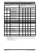
TABLE 30-38: DCI MODULE (MULTI-CHANNEL, I
2
S MODES) TIMING REQUIREMENTS
AC CHARACTERISTICS
Standard Operating Conditions: 3.0V to 3.6V
(unless otherwise stated)
Operating temperature -40°C ≤ TA ≤ +85°C for Industrial
-40°C ≤T
A ≤+125°C for Extended
Param
No.
Symbol Characteristic
(1)
Min Typ
(2)
Max Units Conditions
CS10 TCSCKL CSCK Input Low Time
(CSCK pin is an input)
TCY/2 + 20 — — ns —
CSCK Output Low Time
(3)
(CSCK pin is an output)
30 — — ns —
CS11 TCSCKH CSCK Input High Time
(CSCK pin is an input)
TCY/2 + 20 — — ns —
CSCK Output High Time
(3)
(CSCK pin is an output)
30 — — ns —
CS20 T
CSCKF CSCK Output Fall Time
(4)
(CSCK pin is an output)
—1025ns —
CS21 TCSCKR CSCK Output Rise Time
(4)
(CSCK pin is an output)
—1025ns —
CS30 T
CSDOF CSDO Data Output Fall Time
(4)
—1025ns —
CS31 TCSDOR CSDO Data Output Rise Time
(4)
—1025ns —
CS35 T
DV Clock Edge to CSDO Data Valid — — 10 ns —
CS36 T
DIV Clock Edge to CSDO Tri-Stated 10 — 20 ns —
CS40 TCSDI Setup Time of CSDI Data Input to
CSCK Edge (CSCK pin is input
or output)
20 — — ns —
CS41 THCSDI Hold Time of CSDI Data Input to
CSCK Edge (CSCK pin is input
or output)
20 — — ns —
CS50 TCOFSF COFS Fall Time
(COFS pin is output)
—1025nsSee Note 1
CS51 T
COFSR COFS Rise Time
(COFS pin is output)
—1025nsSee Note 1
CS55 TSCOFS Setup Time of COFS Data Input
to CSCK Edge (COFS pin is
input)
20 — — ns —
CS56 T
HCOFS Hold Time of COFS Data Input to
CSCK Edge (COFS pin is input)
20 — — ns —
Note 1: These parameters are characterized but not tested in manufacturing.
2: Data in “Typ” column is at 3.3V, 25°C unless otherwise stated. Parameters are for design guidance only
and are not tested.
3: The minimum clock period for CSCK is 100 ns. Therefore, the clock generated in Master mode must not
violate this specification.
4: Assumes 50 pF load on all DCI pins.