
Datasheet


dsPIC33FJ32GP302/304, dsPIC33FJ64GPX02/X04, AND dsPIC33FJ128GPX02/X04
DS70292G-page 360 © 2007-2012 Microchip Technology Inc.
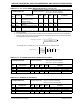
TABLE 30-29: SPIx MASTER MODE (HALF-DUPLEX, TRANSMIT ONLY) TIMING REQUIREMENTS
AC CHARACTERISTICS
Standard Operating Conditions: 3.0V to 3.6V
(unless otherwise stated)
Operating temperature -40°C ≤ TA ≤ +85°C for Industrial
-40°C ≤T
A ≤+125°C for Extended
Param
No.
Symbol Characteristic
(1)
Min Typ
(2)
Max Units Conditions
SP10 TscP Maximum SCK Frequency — — 15 MHz
See Note 3
SP20 TscF SCKx Output Fall Time — — — ns See parameter DO32
and Note 4
SP21 TscR SCKx Output Rise Time — — — ns See parameter DO31
and Note 4
SP30 TdoF SDOx Data Output Fall Time — — — ns See parameter DO32
and Note 4
SP31 TdoR SDOx Data Output Rise Time — — — ns See parameter DO31
and Note 4
SP35 TscH2doV,
TscL2doV
SDOx Data Output Valid after
SCKx Edge
—620ns —
SP36 TdiV2scH,
TdiV2scL
SDOx Data Output Setup to
First SCKx Edge
30 — — ns —
Note 1: These parameters are characterized, but are not tested in manufacturing.
2: Data in “Typ” column is at 3.3V, 25°C unless otherwise stated.
3: The minimum clock period for SCKx is 66.7 ns. Therefore, the clock generated in Master mode must not
violate this specification.
4: Assumes 50 pF load on all SPIx pins.