
Datasheet


© 2007-2012 Microchip Technology Inc. DS70292G-page 319
dsPIC33FJ32GP302/304, dsPIC33FJ64GPX02/X04, AND dsPIC33FJ128GPX02/X04
27.2 On-Chip Voltage Regulator
All of the dsPIC33FJ32GP302/304,
dsPIC33FJ64GPX02/X04, and dsPIC33FJ128GPX02/
X04 devices power their core digital logic at a nominal
2.5V. This can create a conflict for designs that are
required to operate at a higher typical voltage, such as
3.3V. To simplify system design, all devices in the
dsPIC33FJ32GP302/304, dsPIC33FJ64GPX02/X04,
and dsPIC33FJ128GPX02/X04 family incorporate an
on-chip regulator that allows the device to run its core
logic from V
DD.
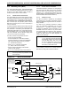
The regulator provides power to the core from the other
V
DD pins. When the regulator is enabled, a low-ESR
(less than 5 Ohms) capacitor (such as tantalum or
ceramic) must be connected to the V
CAP pin
(Figure 27-1). This helps to maintain the stability of the
regulator. The recommended value for the filter capac-
itor is provided in Table 30-13 located in Section 30.1
“DC Characteristics”.
On a POR
, it takes approximately 20 μs for the on-chip
voltage regulator to generate an output voltage. During
this time, designated as TSTARTUP, code execution is
disabled. T
STARTUP is applied every time the device
resumes operation after any power-down.
FIGURE 27-1: CONNECTIONS FOR THE
ON-CHIP VOLTAGE
REGULATOR
(1,2,3)
27.3 BOR: Brown-out Reset
The Brown-out Reset (BOR) module is based on an
internal voltage reference circuit that monitors the reg-
ulated supply voltage V
CAP. The main purpose of the
BOR module is to generate a device Reset when a
brown-out condition occurs. Brown-out conditions are
generally caused by glitches on the AC mains (for
example, missing portions of the AC cycle waveform
due to bad power transmission lines, or voltage sags
due to excessive current draw when a large inductive
load is turned on).
A BOR generates a Reset pulse, which resets the
device. The BOR selects the clock source, based on
the device Configuration bit values (FNOSC<2:0> and
POSCMD<1:0>).
If an oscillator mode is selected, the BOR activates the
Oscillator Start-up Timer (OST). The system clock is
held until OST expires. If the PLL is used, the clock is
held until the LOCK bit (OSCCON<5>) is ‘1’.
Concurrently, the PWRT time-out (TPWRT) is applied
before the internal Reset is released. If TPWRT = 0 and
a crystal oscillator is being used, then a nominal delay
of TFSCM = 100 is applied. The total delay in this case
is TFSCM.
The BOR Status bit (RCON<1>) is set to indicate that a
BOR has occurred. The BOR circuit continues to oper-
ate while in Sleep or Idle modes and resets the device
should VDD fall below the BOR threshold voltage.
Note: It is important for the low-ESR capacitor to
be placed as close as possible to the V
CAP
pin.
Note 1: These are typical operating voltages. Refer to
Table 30-13, located in Section 30.1 “DC
Characteristics” for the full operating ranges
of V
DD and VCAP.
2: It is important for the low-ESR capacitor to be
placed as close as possible to the V
CAP pin.
3: Typical V
CAP pin voltage = 2.5V when
V
DD ≥ VDDMIN.
VDD
VCAP
VSS
dsPIC33F
CEFC
3.3V
10 µF
Tantalum