
Datasheet


© 2007-2012 Microchip Technology Inc. DS70292G-page 315
dsPIC33FJ32GP302/304, dsPIC33FJ64GPX02/X04, AND dsPIC33FJ128GPX02/X04
27.0 SPECIAL FEATURES
dsPIC33FJ32GP302/304, dsPIC33FJ64GPX02/X04,
and dsPIC33FJ128GPX02/X04 devices include
several features intended to maximize application
flexibility and reliability, and minimize cost through
elimination of external components. These are:
• Flexible configuration
• Watchdog Timer (WDT)
• Code Protection and CodeGuard™ Security
• JTAG Boundary Scan Interface
• In-Circuit Serial Programming™ (ICSP™)
• In-Circuit emulation
27.1 Configuration Bits
The dsPIC33FJ32GP302/304, dsPIC33FJ64GPX02/
X04, and dsPIC33FJ128GPX02/X04 devices provide
nonvolatile memory implementation for device
configuration bits. Refer to Section 25. “Device Con-
figuration” (DS70194), in the “dsPIC33F/PIC24H
Family Reference Manual” for more information on this
implementation.
The Configuration bits can be programmed (read as
‘0’), or left unprogrammed (read as ‘1’), to select vari-
ous device configurations. These bits are mapped
starting at program memory location 0xF80000.
The individual Configuration bit descriptions for the
Configuration registers are shown in Table 27-2.
Note that address 0xF80000 is beyond the user program
memory space. It belongs to the configuration memory
space (0x800000-0xFFFFFF), which can only be
accessed using table reads and table writes.
The Device Configuration register map is shown in
Table 27-1.
Note 1: This data sheet summarizes the features
of the dsPIC33FJ32GP302/304,
dsPIC33FJ64GPX02/X04, and
dsPIC33FJ128GPX02/X04 families of
devices. It is not intended to be a compre-
hensive reference source. To comple-
ment the information in this data sheet,
refer to the “dsPIC33F/PIC24H Family
Reference Manual”. Please see the
Microchip web site (www.microchip.com)
for the latest dsPIC33F/PIC24H Family
Reference Manual sections.
2: Some registers and associated bits
described in this section may not be avail-
able on all devices. Refer to Section 4.0
“Memory Organization” in this data
sheet for device-specific register and bit
information.
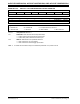
TABLE 27-1: DEVICE CONFIGURATION REGISTER MAP
Address Name Bit 7 Bit 6 Bit 5 Bit 4 Bit 3 Bit 2 Bit 1 Bit 0
0xF80000 FBS RBS<1:0> — — BSS<2:0> BWRP
0xF80002 FSS
(1)
RSS<1:0> — — SSS<2:0> SWRP
0xF80004 FGS
— — — — — GSS<1:0> GWRP
0xF80006 FOSCSEL IESO
— — —FNOSC<2:0>
0xF80008 FOSC FCKSM<1:0> IOL1WAY
— — OSCIOFNC POSCMD<1:0>
0xF8000A FWDT FWDTEN WINDIS — WDTPRE WDTPOST<3:0>
0xF8000C FPOR Reserved
(2)
ALTI2C —FPWRT<2:0>
0xF8000E FICD Reserved
(3)
JTAGEN — — —ICS<1:0>
0xF80010 FUID0 User Unit ID Byte 0
0xF80012 FUID1 User Unit ID Byte 1
0xF80014 FUID2 User Unit ID Byte 2
0xF80016 FUID3 User Unit ID Byte 3
Legend: — = unimplemented bit, read as ‘0’.
Note 1: This Configuration register is not available and reads as 0xFF on dsPIC33FJ32GP302/304 devices.
2: These bits are reserved and always read as ‘1’.
3: These bits are reserved for use by development tools and must be programmed as ‘1’.