
Datasheet


dsPIC33FJ32GP302/304, dsPIC33FJ64GPX02/X04, AND dsPIC33FJ128GPX02/X04
DS70292G-page 290 © 2007-2012 Microchip Technology Inc.
24.1 RTCC Module Registers
The RTCC module registers are organized into three
categories:
• RTCC Control Registers
• RTCC Value Registers
• Alarm Value Registers
24.1.1 REGISTER MAPPING
To limit the register interface, the RTCC Timer and
Alarm Time registers are accessed through corre-
sponding register pointers. The RTCC Value register
window (RTCVALH and RTCVALL) uses the RTCPTR
bits (RCFGCAL<9:8>) to select the desired timer
register pair (see Table 24-1).
By writing the RTCVALH byte, the RTCC Pointer value,
RTCPTR<1:0> bits, decrement by one until they reach
‘00’. Once they reach ‘00’, the MINUTES and
SECONDS value will be accessible through RTCVALH
and RTCVALL until the pointer value is manually
changed.
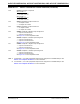
TABLE 24-1: RTCVAL REGISTER MAPPING
The Alarm Value register window (ALRMVALH and
ALRMVALL) uses the ALRMPTR bits
(ALCFGRPT<9:8>) to select the desired Alarm register
pair (see Table 24-2).
By writing the ALRMVALH byte, the Alarm Pointer
value, ALRMPTR<1:0> bits, decrement by one until
they reach ‘00’. Once they reach ‘00’, the ALRMMIN
and ALRMSEC value will be accessible through
ALRMVALH and ALRMVALL until the pointer value is
manually changed.
TABLE 24-2: ALRMVAL REGISTER
MAPPING
Considering that the 16-bit core does not distinguish
between 8-bit and 16-bit read operations, the user must
be aware that when reading either the ALRMVALH or
ALRMVALL bytes will decrement the ALRMPTR<1:0>
value. The same applies to the RTCVALH or RTCVALL
bytes with the RTCPTR<1:0> being decremented.
24.1.2 WRITE LOCK
In order to perform a write to any of the RTCC Timer
registers, the RTCWREN bit (RCFGCAL<13>) must be
set (refer to Example 24-1).
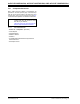
EXAMPLE 24-1: SETTING THE RTCWREN BIT
RTCPTR
<1:0>
RTCC Value Register Window
RTCVAL<15:8> RTCVAL<7:0>
00 MINUTES SECONDS
01 WEEKDAY HOURS
10 MONTH DAY
11 — YEAR
ALRMPTR
<1:0>
Alarm Value Register Window
ALRMVAL<15:8> ALRMVAL<7:0>
00 ALRMMIN ALRMSEC
01 ALRMWD ALRMHR
10 ALRMMNTH ALRMDAY
11 ——
Note: This only applies to read operations and
not write operations.
Note: To avoid accidental writes to the timer, it is
recommended that the RTCWREN bit
(RCFGCAL<13>) is kept clear at any
other time. For the RTCWREN bit to be
set, there is only 1 instruction cycle time
window allowed between the 55h/AA
sequence and the setting of RTCWREN;
therefore, it is recommended that code
follow the procedure in Example 24-1.
MOV #NVMKEY, W1 ;move the address of NVMKEY into W1
MOV #0x55, W2
MOV #0xAA, W3
MOV W2, [W1] ;start 55/AA sequence
MOV W3, [W1]
BSET RCFGCAL, #13 ;set the RTCWREN bit