
Datasheet


dsPIC33FJ32GP302/304, dsPIC33FJ64GPX02/X04, AND dsPIC33FJ128GPX02/X04
DS70292G-page 278 © 2007-2012 Microchip Technology Inc.
22.4 DAC Clock
The DAC clock signal clocks the internal logic of the
Audio DAC module. The data sample rate of the Audio
DAC is an integer division of the rate of the DAC clock.
The DAC clock is generated via a clock divider circuit
that accepts an auxiliary clock from the auxiliary
oscillator.
The divisor ratio is programmed by clock divider bits
(DACFDIV<6:0>) in the DAC Control register
(DAC1CON). The resulting DAC clock must not exceed
25.6 MHz. If lower sample rates are to be used, then
the DAC filter clock frequency may be reduced to
reduce power consumption. The DAC clock frequency
is 256 times the sampling frequency.
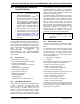
FIGURE 22-1: BLOCK DIAGRAM OF AUDIO DIGITAL-TO-ANALOG (DAC) CONVERTER
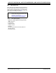
FIGURE 22-2: AUDIO DAC OUTPUT FOR RAMP INPUT (UNSIGNED)
DAC1RDAT
DAC1LDAT
D/A
D/A
CONTROL
CLK DIV
DACDFLT
Amp
16-bit Data Bus
Amp
ACLK
Note 1: If DAC1RDAT and DAC1LDAT are empty, data will be taken from the DACDFLT register.
Note 1
Note 1
DAC1LM
DAC1LP
DAC1LN
DAC1RM
DAC1RP
DAC1RN
Right Channel
Left Channel
DACFDIV<6:0>
0x0000
0xFFFF
DAC input
Count (DAC1RDAT)
VDACM
VDACM
Positive DAC
Output (DAC1RP)
Negative DAC
Output (DAC1RN)
VDACH
VDACL
VDACL
VDACH
Note: VOD+ = VDACH – VDACL, VOD- = VDACL – VDACH; refer to Audio DAC Module Specifications, Table 30-46, for typical values.