
Datasheet


dsPIC33FJ32GP302/304, dsPIC33FJ64GPX02/X04, AND dsPIC33FJ128GPX02/X04
DS70292G-page 212 © 2007-2012 Microchip Technology Inc.
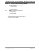
REGISTER 16-3: SPIxCON2: SPIx CONTROL REGISTER 2
R/W-0 R/W-0 R/W-0 U-0 U-0 U-0 U-0 U-0
FRMEN SPIFSD FRMPOL
— — — — —
bit 15 bit 8
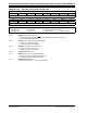
U-0 U-0 U-0 U-0 U-0 U-0 R/W-0 U-0
— — — — — — FRMDLY —
bit 7 bit 0
Legend:
R = Readable bit W = Writable bit U = Unimplemented bit, read as ‘0’
-n = Value at POR ‘1’ = Bit is set ‘0’ = Bit is cleared x = Bit is unknown
bit 15 FRMEN: Framed SPIx Support bit
1 = Framed SPIx support enabled (SSx
pin used as frame sync pulse input/output)
0 = Framed SPIx support disabled
bit 14 SPIFSD: Frame Sync Pulse Direction Control bit
1 = Frame sync pulse input (slave)
0 = Frame sync pulse output (master)
bit 13 FRMPOL: Frame Sync Pulse Polarity bit
1 = Frame sync pulse is active-high
0 = Frame sync pulse is active-low
bit 12-2 Unimplemented: Read as ‘0’
bit 1 FRMDLY: Frame Sync Pulse Edge Select bit
1 = Frame sync pulse coincides with first bit clock
0 = Frame sync pulse precedes first bit clock
bit 0 Unimplemented: Read as ‘0’
This bit must not be set to ‘1’ by the user application.