
Datasheet


dsPIC33FJ32GP302/304, dsPIC33FJ64GPX02/X04, AND dsPIC33FJ128GPX02/X04
DS70292G-page 204 © 2007-2012 Microchip Technology Inc.
15.1 Output Compare Modes
Configure the Output Compare modes by setting the
appropriate Output Compare Mode bits (OCM<2:0>) in
the Output Compare Control register (OCxCON<2:0>).
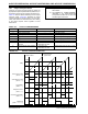
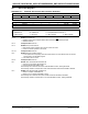
Table 15-1 lists the different bit settings for the Output
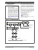
Compare modes. Figure 15-2 illustrates the output
compare operation for various modes. The user appli-
cation must disable the associated timer when writing
to the output compare control registers to avoid
malfunctions.
TABLE 15-1: OUTPUT COMPARE MODES
FIGURE 15-2: OUTPUT COMPARE OPERATION
Note 1: Only OC1 and OC2 can trigger a DMA
data transfer.
2: See Section 13. “Output Compare”
(DS70209) in the “dsPIC33F/PIC24H
Family Reference Manual” for OCxR and
OCxRS register restrictions.
OCM<2:0> Mode OCx Pin Initial State OCx Interrupt Generation
000 Module Disabled Controlled by GPIO register —
001 Active-Low One-Shot 0 OCx Rising edge
010 Active-High One-Shot 1 OCx Falling edge
011 Toggle Mode Current output is maintained OCx Rising and Falling edge
100 Delayed One-Shot 0 OCx Falling edge
101 Continuous Pulse mode 0 OCx Falling edge
110 PWM mode without fault
protection
0, if OCxR is zero
1, if OCxR is non-zero
No interrupt
111 PWM mode with fault protection 0, if OCxR is zero
1, if OCxR is non-zero
OCFA
Falling edge for OC1 to OC4
OCxRS
TMRy
OCxR
Timer is reset on
period match
Continuous Pulse Mode
(OCM = 101)
PWM Mode
(OCM = 110 or 111)
Active-Low One-Shot
(OCM = 001)
Active-High One-Shot
(OCM = 010)
Toggle Mode
(OCM = 011)
Delayed One-Shot
(OCM = 100)
Output Compare
Mode enabled