
Datasheet


dsPIC33FJ32GP302/304, dsPIC33FJ64GPX02/X04, AND dsPIC33FJ128GPX02/X04
DS70292G-page 20 © 2007-2012 Microchip Technology Inc.
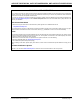
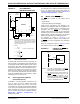
FIGURE 2-1: RECOMMENDED
MINIMUM CONNECTION
2.2.1 TANK CAPACITORS
On boards with power traces running longer than six
inches in length, it is suggested to use a tank capacitor
for integrated circuits including DSCs to supply a local
power source. The value of the tank capacitor should
be determined based on the trace resistance that con-
nects the power supply source to the device, and the
maximum current drawn by the device in the applica-
tion. In other words, select the tank capacitor so that it
meets the acceptable voltage sag at the device. Typical
values range from 4.7 µF to 47 µF.
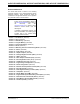
2.3 CPU Logic Filter Capacitor
Connection (V
CAP)
A low-ESR (< 5 Ohms) capacitor is required on the
V
CAP pin, which is used to stabilize the voltage
regulator output voltage. The VCAP pin must not be
connected to VDD, and must have a capacitor between
4.7 µF and 10 µF, preferably surface mount connected
within one-eights inch of the V
CAP pin connected to
ground. The type can be ceramic or tantalum. Refer to
Section 30.0 “Electrical Characteristics” for
additional information.
The placement of this capacitor should be close to the
VCAP. It is recommended that the trace length not
exceed one-quarter inch (6 mm). Refer to Section 27.2
“On-Chip Voltage Regulator” for details.
2.4 Master Clear (MCLR) Pin
The MCLR pin provides for two specific device
functions:
• Device Reset
• Device programming and debugging
During device programming and debugging, the
resistance and capacitance that can be added to the
pin must be considered. Device programmers and
debuggers drive the MCLR
pin. Consequently,
specific voltage levels (VIH and VIL) and fast signal
transitions must not be adversely affected. Therefore,
specific values of R and C will need to be adjusted
based on the application and PCB requirements.
For example, as shown in Figure 2-2, it is
recommended that the capacitor C, be isolated from
the MCLR
pin during programming and debugging
operations.
Place the components shown in Figure 2-2 within
one-quarter inch (6 mm) from the MCLR
pin.
FIGURE 2-2: EXAMPLE OF MCLR PIN
CONNECTIONS
dsPIC33F
VDD
VSS
VDD
VSS
VSS
VDD
AVDD
AVSS
VDD
VSS
0.1 µF
Ceramic
0.1 µF
Ceramic
0.1 µF
Ceramic
0.1 µF
Ceramic
C
R
V
DD
MCLR
0.1 µF
Ceramic
VCAP
L1
(1)
R1
10 µF
Tantalum
Note 1: As an option, instead of a hard-wired connection, an
inductor (L1) can be substituted between V
DD and
AV
DD to improve ADC noise rejection. The inductor
impedance should be less than 1Ω and the inductor
capacity greater than 10 mA.
Where:
f
FCNV
2
--------------=
f
1
2π LC()
-----------------------=
L
1
2πfC()
---------------------
⎝⎠
⎛⎞
2
=
(i.e., ADC conversion rate/2)
Note 1: R ≤ 10 kΩ is recommended. A suggested
starting value is 10 kΩ. Ensure that the MCLR
pin VIH and VIL specifications are met.
2: R1 ≤ 470Ω will limit any current flowing into
MCLR
from the external capacitor C, in the
event of MCLR
pin breakdown, due to
Electrostatic Discharge (ESD) or Electrical
Overstress (EOS). Ensure that the MCLR
pin
V
IH and VIL specifications are met.
C
R1
(2)
R
(1)
VDD
MCLR
dsPIC33F
JP