
Datasheet


© 2007-2012 Microchip Technology Inc. DS70292G-page 189
dsPIC33FJ32GP302/304, dsPIC33FJ64GPX02/X04, AND dsPIC33FJ128GPX02/X04
12.0 TIMER1
The Timer1 module is a 16-bit timer, which can serve
as the time counter for the real-time clock, or operate
as a free-running interval timer/counter.
The Timer1 module has the following unique features
over other timers:
• Can be operated from the low power 32 kHz
crystal oscillator available on the device
• Can be operated in Asynchronous Counter mode
from an external clock source.
• The external clock input (T1CK) can optionally be
synchronized to the internal device clock and the
clock synchronization is performed after the
prescaler.
The unique features of Timer1 allow it to be used for
Real-Time Clock (RTC) applications. A block diagram
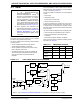
of Timer1 is shown in Figure 12-1.
The Timer1 module can operate in one of the following
modes:
• Timer mode
• Gated Timer mode
• Synchronous Counter mode
• Asynchronous Counter mode
In Timer and Gated Timer modes, the input clock is
derived from the internal instruction cycle clock (F
CY).
In Synchronous and Asynchronous Counter modes,
the input clock is derived from the external clock input
at the T1CK pin.
The Timer modes are determined by the following bits:
• Timer Clock Source Control bit (TCS): T1CON<1>
• Timer Synchronization Control bit (TSYNC):
T1CON<2>
• Timer Gate Control bit (TGATE): T1CON<6>
Timer control bit setting for different operating modes
are given in the Table 12-1.
TABLE 12-1: TIMER MODE SETTINGS
FIGURE 12-1: 16-BIT TIMER1 MODULE BLOCK DIAGRAM
Note 1: This data sheet summarizes the features
of the dsPIC33FJ32GP302/304,
dsPIC33FJ64GPX02/X04, and
dsPIC33FJ128GPX02/X04 families of
devices. It is not intended to be a compre-
hensive reference source. To comple-
ment the information in this data sheet,
refer to Section 11. “Timers” (DS70205)
of the “dsPIC33F/PIC24H Family Refer-
ence Manual”, which is available from the
Microchip website (www.microchip.com).
2: Some registers and associated bits
described in this section may not be avail-
able on all devices. Refer to Section 4.0
“Memory Organization” in this data
sheet for device-specific register and bit
information.
Mode TCS TGATE TSYNC
Timer 00x
Gated timer 01x
Synchronous
counter
1x1
Asynchronous
counter
1x0
TGATE
TCS
00
10
x1
TMR1
Comparator
PR1
TGATE
Set T1IF flag
0
1
TSYNC
1
0
Sync
Equal
Reset
SOSCI
SOSCO/
T1CK
Prescaler
(/n)
TCKPS<1:0>
Gate
Sync
F
CY
Falling Edge
Detect
Prescaler
(/n)
TCKPS<1:0>
LPOSCEN
(1)
Note 1: Refer to Section 9.0 “Oscillator Configuration” for information on enabling the secondary oscillator.