
Datasheet


© 2007-2012 Microchip Technology Inc. DS70292G-page 159
dsPIC33FJ32GP302/304, dsPIC33FJ64GPX02/X04, AND dsPIC33FJ128GPX02/X04
11.0 I/O PORTS
All of the device pins (except VDD, VSS, MCLR and
OSC1/CLKI) are shared among the peripherals and the
parallel I/O ports. All I/O input ports feature Schmitt
Trigger inputs for improved noise immunity.
11.1 Parallel I/O (PIO) Ports
Generally a parallel I/O port that shares a pin with a
peripheral is subservient to the peripheral. The
peripheral’s output buffer data and control signals are
provided to a pair of multiplexers. The multiplexers
select whether the peripheral or the associated port
has ownership of the output data and control signals of
the I/O pin. The logic also prevents “loop through,” in
which a port’s digital output can drive the input of a
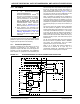
peripheral that shares the same pin. Figure 11-1 shows
how ports are shared with other peripherals and the
associated I/O pin to which they are connected.
When a peripheral is enabled and the peripheral is
actively driving an associated pin, the use of the pin as
a general purpose output pin is disabled. The I/O pin
can be read, but the output driver for the parallel port bit
is disabled. If a peripheral is enabled, but the peripheral
is not actively driving a pin, that pin can be driven by a
port.
All port pins have three registers directly associated
with their operation as digital I/O. The data direction
register (TRISx) determines whether the pin is an input
or an output. If the data direction bit is a ‘1’, then the pin
is an input. All port pins are defined as inputs after a
Reset. Reads from the latch (LATx) read the latch.
Writes to the latch write the latch. Reads from the port
(PORTx) read the port pins, while writes to the port pins
write the latch.
Any bit and its associated data and control registers
that are not valid for a particular device is disabled.
This means the corresponding LATx and TRISx
registers and the port pin are read as zeros.
When a pin is shared with another peripheral or
function that is defined as an input only, it is
nevertheless regarded as a dedicated port because
there is no other competing source of outputs.
FIGURE 11-1: BLOCK DIAGRAM OF A TYPICAL SHARED PORT STRUCTURE
Note 1: This data sheet summarizes the features
of the dsPIC33FJ32GP302/304,
dsPIC33FJ64GPX02/X04, and
dsPIC33FJ128GPX02/X04 families of
devices. It is not intended to be a compre-
hensive reference source. To comple-
ment the information in this data sheet,
refer to Section “30. I/O Ports with
Peripheral Pin Select” (DS70190) of the
“dsPIC33F/PIC24H Family Reference
Manual”, which is available from the
Microchip website (www.microchip.com).
2: Some registers and associated bits
described in this section may not be avail-
able on all devices. Refer to Section 4.0
“Memory Organization” in this data
sheet for device-specific register and bit
information.
QD
CK
WR LAT +
TRIS Latch
I/O Pin
WR Port
Data Bus
QD
CK
Data Latch
Read Port
Read TRIS
1
0
1
0
WR TRIS
Peripheral Output Data
Output Enable
Peripheral Input Data
I/O
Peripheral Module
Peripheral Output Enable
PIO Module
Output Multiplexers
Output Data
Input Data
Peripheral Module Enable
Read LAT