
Datasheet


dsPIC33FJ32GP302/304, dsPIC33FJ64GPX02/X04, AND dsPIC33FJ128GPX02/X04
DS70292G-page 134 © 2007-2012 Microchip Technology Inc.
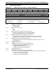
REGISTER 8-3: DMAxSTA: DMA CHANNEL x RAM START ADDRESS REGISTER A
(1)
R/W-0 R/W-0 R/W-0 R/W-0 R/W-0 R/W-0 R/W-0 R/W-0
STA<15:8>
bit 15 bit 8
R/W-0 R/W-0 R/W-0 R/W-0 R/W-0 R/W-0 R/W-0 R/W-0
STA<7:0>
bit 7 bit 0
Legend:
R = Readable bit W = Writable bit U = Unimplemented bit, read as ‘0’
-n = Value at POR ‘1’ = Bit is set ‘0’ = Bit is cleared x = Bit is unknown
bit 15-0 STA<15:0>: Primary DMA RAM Start Address bits (source or destination)
Note 1: A read of this address register returns the current contents of the DMA RAM Address register, not the con-
tents written to STA<15:0>. If the channel is enabled (i.e., active), writes to this register may result in
unpredictable behavior of the DMA channel and should be avoided.
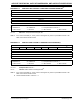
REGISTER 8-4: DMAxSTB: DMA CHANNEL x RAM START ADDRESS REGISTER B
(1)
R/W-0 R/W-0 R/W-0 R/W-0 R/W-0 R/W-0 R/W-0 R/W-0
STB<15:8>
bit 15 bit 8
R/W-0 R/W-0 R/W-0 R/W-0 R/W-0 R/W-0 R/W-0 R/W-0
STB<7:0>
bit 7 bit 0
Legend:
R = Readable bit W = Writable bit U = Unimplemented bit, read as ‘0’
-n = Value at POR ‘1’ = Bit is set ‘0’ = Bit is cleared x = Bit is unknown
bit 15-0 STB<15:0>: Secondary DMA RAM Start Address bits (source or destination)
Note 1: A read of this address register returns the current contents of the DMA RAM Address register, not the con-
tents written to STB<15:0>. If the channel is enabled (i.e., active), writes to this register may result in
unpredictable behavior of the DMA channel and should be avoided.