
Datasheet


© 2007-2012 Microchip Technology Inc. DS70292G-page 129
dsPIC33FJ32GP302/304, dsPIC33FJ64GPX02/X04, AND dsPIC33FJ128GPX02/X04
8.0 DIRECT MEMORY ACCESS
(DMA)
Direct Memory Access (DMA) is a very efficient
mechanism of copying data between peripheral SFRs
(e.g., UART Receive register, Input Capture 1 buffer),
and buffers or variables stored in RAM, with minimal
CPU intervention. The DMA controller can
automatically copy entire blocks of data without
requiring the user software to read or write the
peripheral Special Function Registers (SFRs) every
time a peripheral interrupt occurs. The DMA controller
uses a dedicated bus for data transfers and therefore,
does not steal cycles from the code execution flow of
the CPU. To exploit the DMA capability, the
corresponding user buffers or variables must be
located in DMA RAM.
The dsPIC33FJ32GP302/304, dsPIC33FJ64GPX02/
X04, and dsPIC33FJ128GPX02/X04 peripherals that
can utilize DMA are listed in Table 8-1.
Note 1: This data sheet summarizes the features
of the dsPIC33FJ32GP302/304,
dsPIC33FJ64GPX02/X04, and
dsPIC33FJ128GPX02/X04 families of
devices. It is not intended to be a compre-
hensive reference source. To comple-
ment the information in this data sheet,
refer to Section 38. “Direct Memory
Access (DMA) (Part III)” (DS70215) of
the “dsPIC33F/PIC24H Family Reference
Manual”, which is available from the
Microchip website (www.microchip.com).
2: Some registers and associated bits
described in this section may not be avail-
able on all devices. Refer to Section 4.0
“Memory Organization” in this data
sheet for device-specific register and bit
information.
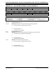
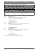
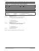
TABLE 8-1: DMA CHANNEL TO PERIPHERAL ASSOCIATIONS
Peripheral to DMA Association
DMAxREQ Register
IRQSEL<6:0> Bits
DMAxPAD Register
Values to Read from
Peripheral
DMAxPAD Register
Values to Write to
Peripheral
INT0 – External Interrupt 0 0000000 ——
IC1 – Input Capture 1 0000001 0x0140 (IC1BUF) —
OC1 – Output Compare 1 Data 0000010 — 0x0182 (OC1R)
OC1 – Output Compare 1 Secondary Data 0000010 — 0x0180 (OC1RS)
IC2 – Input Capture 2 0000101 0x0144 (IC2BUF) —
OC2 – Output Compare 2 Data 0000110 — 0x0188 (OC2R)
OC2 – Output Compare 2 Secondary Data 0000110 — 0x0186 (OC2RS)
TMR2 – Timer2 0000111 ——
TMR3 – Timer3 0001000 ——
SPI1 – Transfer Done 0001010 0x0248 (SPI1BUF) 0x0248 (SPI1BUF)
UART1RX – UART1 Receiver 0001011 0x0226 (U1RXREG) —
UART1TX – UART1 Transmitter 0001100 — 0x0224 (U1TXREG)
ADC1 – ADC1 convert done 0001101 0x0300 (ADC1BUF0) —
UART2RX – UART2 Receiver 0011110 0x0236 (U2RXREG) —
UART2TX – UART2 Transmitter 0011111 — 0x0234 (U2TXREG)
SPI2 – Transfer Done 0100001 0x0268 (SPI2BUF) 0x0268 (SPI2BUF)
ECAN1 – RX Data Ready 0100010 0x0440 (C1RXD) —
PMP – Master Data Transfer 0101101 0x0608 (PMDIN1) 0x0608 (PMDIN1)
ECAN1 – TX Data Request 1000110 — 0x0442 (C1TXD)
DCI – Codec Transfer Done 0111100 0x0290 (RXBUF0) 0x0298 (TXBUF0)
DAC1 – Right Data Output 1001110 — 0x03F6 (DAC1RDAT)
DAC2 – Left Data Output 1001111 — 0x03F8 (DAC1LDAT)