
Specifications

© 2006 Microchip Technology Inc. DS70183A-page 16-9
Section 16. Analog-to-Digital Converter (ADC)
A
D
C
16
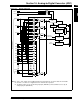
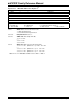
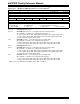
Register 16-4: ADxCON4: ADCx Control Register 4
(1)
U-0 U-0 U-0 U-0 U-0 U-0 U-0 U-0
— — — — — — — —
bit 15 bit 8
U-0 U-0 U-0 U-0 U-0 R/W-0 R/W-0 R/W-0
— — — — — DMABL<2:0>
bit 7 bit 0
Legend:
R = Readable bit W = Writable bit U = Unimplemented bit, read as ‘0’
-n = Value at POR ‘1’ = Bit is set ‘0’ = Bit is cleared x = Bit is unknown
bit 15-3 Unimplemented: Read as ‘0’
bit 2-0 DMABL<2:0>: Selects Number of DMA Buffer Locations per Analog Input bits
111 =Allocates 128 words of buffer to each analog input
110 =Allocates 64 words of buffer to each analog input
101 =Allocates 32 words of buffer to each analog input
100 =Allocates 16 words of buffer to each analog input
011 =Allocates 8 words of buffer to each analog input
010 =Allocates 4 words of buffer to each analog input
001 =Allocates 2 words of buffer to each analog input
000 =Allocates 1 word of buffer to each analog input
Note 1: The ‘x’ in ADxCON4 and ADCx refers to ADC 1 or ADC 2.