
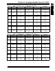
Specifications


dsPIC33F Family Reference Manual
DS70183A-page 16-54 © 2006 Microchip Technology Inc.
16.19 ADC ACCURACY/ERROR
Refer to Section 16.26 “Related Application Notes” for a list of documents that discuss ADC
accuracy.
16.20 CONNECTION CONSIDERATIONS
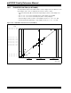
Since the analog inputs employ ESD protection, they have diodes to VDD and VSS. As a result,
the analog input must be between V
DD and VSS. If the input voltage exceeds this range by greater
than 0.3 V (either direction), one of the diodes becomes forward biased, and it may damage the
device if the input current specification is exceeded.
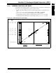
An external RC filter is sometimes added for anti-aliasing of the input signal. The R component
should be selected to ensure that the sampling time requirements are satisfied. Any external
components connected (via high-impedance) to an analog input pin (capacitor, zener diode, etc.)
should have very little leakage current at the pin.
16.21 CODE EXAMPLES
Two code examples that demonstrate typical ADC usage scenarios are described here:
16.21.1 Channel Scanning Using DMA
Example 16-4 configures a DMA channel for storing 32 ADC results in the Scatter/Gather mode.
The ADC is set up to scan four analog inputs (AN0, AN1, AN2, AN3), thereby providing eight
samples of each input in the DMA buffer.
16.21.2 Alternate Sampling Using DMA
Example 16-5 performs alternate sampling of two analog inputs (AN4, AN5) and stores the
results in a 32-word DMA buffer using the Scatter/Gather mode.