
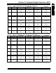
Specifications


dsPIC33F Family Reference Manual
DS70183A-page 16-52 © 2006 Microchip Technology Inc.
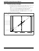
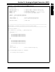
16.17 TRANSFER FUNCTION (10-BIT MODE)
The ideal transfer function of the ADC module is shown in Figure 16-27. The difference of the
input voltages, (V
INH – VINL), is compared to the reference, (VREFH – VREFL).
• The first code transition (A) occurs when the input voltage is (V
REFH – VREFL/2048) or 0.5
LSb.
•The 00 0000 0001 code is centered at (V
REFH – VREFL/1024) or 1.0 LSb (B).
•The 10 0000 0000 code is centered at (512*(V
REFH – VREFL)/1024) (C).
• An input voltage less than (1*(VREFH – VREFL)/2048) converts as 00 0000 0000 (D).
• An input greater than (2045*(VREFH – VREFL)/2048) converts as 11 1111 1111 (E).
Figure 16-27: ADC Module Transfer Function (10-bit Mode)
10 0000 0010 (= 514)
10 0000 0011 (= 515)
01 1111 1101 (= 509)
01 1111 1110 (= 510)
01 1111 1111 (= 511)
11 1111 1110 (= 1022)
11 1111 1111 (= 1023)
00 0000 0000 (= 0)
00 0000 0001 (= 1)
Output
Code
10 0000 0000 (= 512)
(VINH – VINL)
V
REFL
VREFH – VREFL
1024
VREFH
VREFL +
10 0000 0001 (= 513)
512*(VREFH – VREFL)
1024
VREFL +
1023*(V
REFH – VREFL)
1024
VREFL +
(A)
(B)
(C)
(D)
(E)