
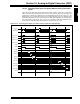
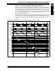
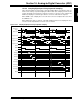
Specifications


© 2006 Microchip Technology Inc. DS70183A-page 16-49
Section 16. Analog-to-Digital Converter (ADC)
A
D
C
16
16.15 A/D SAMPLING REQUIREMENTS
The analog input model of the 10-bit and 12-bit ADC modes are shown in Figure 16-23 and
Figure 16-24. The total sampling time for the A/D conversion is a function of the internal amplifier
settling time and the holding capacitor charge time.
For the ADC module to meet its specified accuracy, the charge holding capacitor (C
HOLD) must
be allowed to fully charge to the voltage level on the analog input pin. The analog output source
impedance (RS), the interconnect impedance (RIC) and the internal sampling switch (RSS)
impedance combine to directly affect the time required to charge the capacitor C
HOLD. The com-
bined impedance must, therefore, be small enough to fully charge the holding capacitor within
the chosen sample time. To minimize the effects of pin leakage currents on the accuracy of the
ADC module, the maximum recommended source impedance, R
S, is 200Ω. After the analog
input channel is selected, this sampling function must be completed prior to starting the conver-
sion. The internal holding capacitor will be in a discharged state prior to each sample operation.
A minimum time period should be allowed between conversions for the sample time. For more
details about the minimum sampling time for a device, see the device electrical specifications.
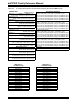
Figure 16-23: Analog Input Model (10-bit Mode)
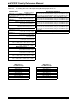
Figure 16-24: Analog Input Model (12-bit Mode)
CPIN
VA
Rs
ANx
V
T = 0.6V
VT = 0.6V
I leakage
R
IC ≤ 250Ω
Sampling
Switch
R
SS
CHOLD
= DAC capacitance
V
SS
VDD
= 4.4 pF
± 500 nA
Legend: CPIN
VT
I leakage
R
IC
RSS
CHOLD
= input capacitance
= threshold voltage
= leakage current at the pin due to
= interconnect resistance
= sampling switch resistance
= Sample/Hold capacitance (from DAC)
various junctions
Note: CPIN value depends on device package and is not tested. Effect of CPIN negligible if Rs ≤ 500Ω.
R
SS ≤ 3 kΩ
CPIN
VA
Rs
ANx
V
T = 0.6V
VT = 0.6V
I leakage
R
IC ≤ 250Ω
Sampling
Switch
R
SS
CHOLD
= DAC capacitance
V
SS
VDD
= 18 pF
± 500 nA
Legend: CPIN
VT
I leakage
R
IC
RSS
CHOLD
= input capacitance
= threshold voltage
= leakage current at the pin due to
= interconnect resistance
= sampling switch resistance
= Sample/Hold capacitance (from DAC)
various junctions
Note: CPIN value depends on device package and is not tested. Effect of CPIN negligible if Rs ≤ 5 kΩ.
R
SS ≤ 3 kΩ