
Specifications


© 2006 Microchip Technology Inc. DS70183A-page 16-43
Section 16. Analog-to-Digital Converter (ADC)
A
D
C
16
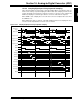
16.14.4 Using Alternating MUX A, MUX B Input Selections
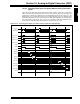
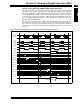
Figure 16-20 and Table 16-5 demonstrate alternate sampling of the inputs assigned to MUX A
and MUX B. In this example, two channels are enabled to sample simultaneously. Setting the
ALTS bit (ADCxCON2<0>) enables alternating input selections. The first sample uses the MUX
A inputs specified by the CH0SA, CH0NA, CH123SA and CH123NA bits. The next sample uses
the MUX B inputs specified by the CH0SB, CH0NB, CH123SB and CH123NB bits. In this exam-
ple, one of the MUX B input specifications uses two analog inputs as a differential source to the
Sample/Hold, sampling (AN3-AN9).
Note that using four Sample/Hold channels without alternating input selections results in the
same number of conversions as this example, using two channels with alternating input selec-
tions. However, because the CH1, CH2 and CH3 channels are more limited in the selectivity of
the analog inputs, this example method provides more flexibility of input selection than using four
channels.
Figure 16-20: Converting Two Sets of Two Inputs Using Alternating Input Selections
ADC Clock
SAMP
Buffer[0]
Buffer[1]
DONE
Buffer[2]
Buffer[3]
Input to
AN1
TSAMP
ADxIF
TCONVTCONV
AN0
Input to
Buffer[4]
Buffer[5]
Buffer[6]
Buffer[7]
AN15
TSAMP
TCONVTCONV
AN3-AN9
ASAM
BUFS
AN1
TSAMP
TCONVTCONV
AN0
AN15
TSAMP
TCONVTCONV
AN3-AN9
Buffer[8]
TCONVTCONV
TSAMP
AN15
AN3-AN9
Cleared by Software
CH0
CH1
Conversion
Trigger
Cleared
in software